Electron backscattering diffraction (EBSD) / technique used in the scanning and transmission microscope Part # 2 (preparation of material)
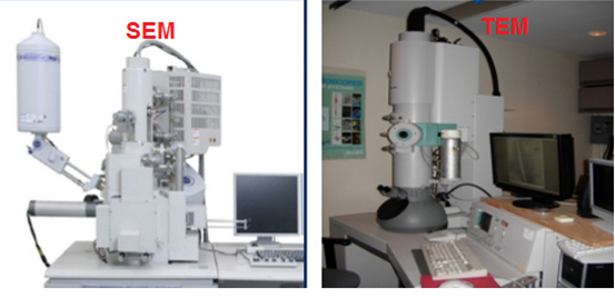
In the previous post explain a new technique of structural characterization of materials called EBSD. Used by means of microscopes, either scanning or transmission, this allows to determine material surfaces, grain size, as well as crystalline phases by means of diffraction patterns, in the same way in this type of characterization we can observe the calls Kikuchi lines that are presented on the surface of the materials studied, this technique basically consists of the interaction of the electron beam on the sample and it is said that they are of low energy because when they hit the material, the electrons lose a large part of energy and that is why you can observe different studies of the material and the great advantage as explained above is that you can incorporate both the SEM as to TEM.
Source
Now then in this publication I want to show you how to prepare a sample of any material you want to characterize by means of this technique, this I do in order to clarify doubts about the subject under discussion.
In particular I have not prepared a sample to perform this technique I have only observed the laboratory staff, but basically the method of preparation is very similar to the post I explained several weeks ago, which shows how a sample is prepared to characterize optics and electrically see here. Although I have not yet entered electrical and optical matter I wanted to make that publication because at that precise moment I was working on it and decided to write the post, as in this case we are still discussing the structural part I would not like to deviate so much, later I will talk about the optical and electrical part of semiconductors.
When we want to characterize a material using the EBSD technique, we must prepare them very carefully and this is because this technique is very sensitive to superficial defects on the sample, that is, if the sample is full of corrosion or some other defect. measures will not turn out as we wish.
To avoid topographical effects, ie, that the sample is rough and obtain a diffractogram showing strong intensity lines, first we must clean the sample well, eliminate all possible rust or corrosion, normally this happens when the samples spend a lot of time saved after its growth and were not encapsulated correctly. To eliminate this corrosion effect we must immerse the sample in a glass container filled with ethyl alcohol or if in the laboratory we have chloroform available it would be excellent, since it is a much stronger chemical and completely eliminates the oxide, we leave the sample approximately 12 hours Inside the container, after that time we remove it and let it air dry for about 30 minutes.
Later if the ingot of the sample is deformed we can give uniformity using sandpapers (see figure 2) to reduce said sample and leave it completely on its surfaces, since this technique only allows the electron beam to penetrate the surfaces of the material, more not in its depth.
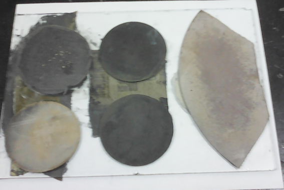
Figure 2. Different types of sandpaper used to reduce the size of samples of semiconductor compounds.
If we want to get the patterns of Kikuchi quite strong (see figure 3 and 4), that is to say that the lines are seen clearly we must eliminate all the corrosion possible and deformation in the sample.
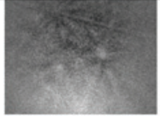
Figure 3. Kikuchi lines (1).
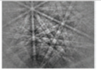
Figure 4. Kikuchi lines (1).
Figures 3 and 4 show the great difference that exists when a sample of a material to be characterized by means of this technique is not prepared correctly and there are problems when visualizing the Kikuchi lines, in the figure 3 the material was deformed or with a little corrosion, however in figure 4 the material is prepared correctly and the lines are observed quite clearly.
The most important thing so that there are no weak patterns is to mount the sample in a bakelite (see figure 5) to facilitate handling when polishing, you can polish manually using different cloths and a liquid called alumina that allows the sample It looks bright, but it is advisable to use an automatic polisher (see figure 6) to polish the material and thus ensure greater cleaning and effective cleaning.
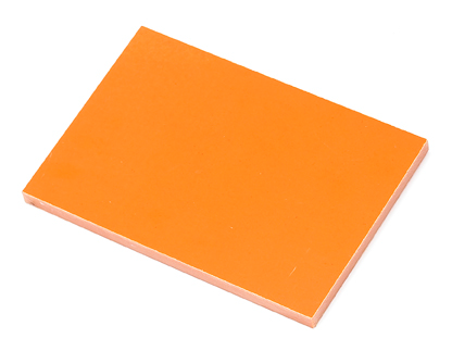
Figure 5. Bakelite.
Source
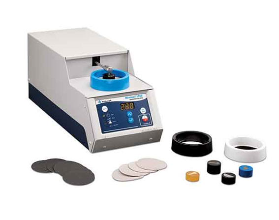
Figure 6. Instrument used to polish samples of semiconductor materials (polishing and devastating).
Source
It is also recommended to polish electrochemically, ionically or chemically, and let the sample rest in vacuum to avoid the formation of any undesired oxide or substance, which may adhere to the surface and cause problems in the results.
The EBSD technique is very important to characterize materials, both qualitatively and quantitatively, it shows us that we can study all the aspects related in part structure and crystallography of the science of materials. It is a very useful tool to determine phases in materials, grain size, atomic positions, texture, among others. The indexation by means of diffraction patterns allows to obtain a reliable analysis of results.
In addition to being a very versatile technique, it helps us apply it in different branches of science and when we say versatile it is that we can use it in SEM as well as in TEM.
It should be noted that this technique also presents a difficult handle as it requires very stealthy preventive measures when characterizing a sample, since its preparation is very delicate and if not done correctly the results will be incorrect, it is recommended to wear gloves, mask protective, and appropriate clothing when preparing the sample because any additional effect on it can alter the results.
References:
(1) My publication was supported by the article by Dairo Hernán Mesa Grajales: Principles and applications of the Electron Back-Scattering Diffraction Technical (EBSD). Curriculum
https://www.slideshare.net/kalyanacharjya/electron-microscopy-sem-tem
If you want to see more about electron microscopy visit my previous publications:
And if you want to learn a bit about semiconductors you can also visit the following publications:
You kept your word and you made the post, thanks man!
I am a man of my word, the promised is fulfilled friend :D