Do you know semiconductors? your answer is no... "I will explain to you very easily"
As I mentioned in my post introduction, I am a physics student, I am practically already graduating; I am finishing my thesis in the area of physics of materials, specifically study the semiconductor compounds. Conducting experimental studies of structural, optical and electrical character. But before talking with details of what it is all about, the first thing is to start from the base such as knowing that it is a semiconductor.

Figure 1. Image source: https://www.swagelok.com/es-ES/Industries/Semiconductor.
To speak from my perspective and knowledge in the area, I could tell you that a semiconductor compound; is one that can behave as a conductor or insulation, depending on different factors such as; temperature, pressure, some electric or magnetic field. These semiconductor compounds can be silicon or germanium which are the most abundant in the earth. The semiconductors are elements of the periodic table that can be combined, that is to say by means of different techniques of growth, a synthesis can be made and to form a ternary compound like for example CuInSe or CuInTe, that are the most used for the manufacture of prototypes of solar cells. These elements have an electrical conductivity lower than that of metals but superior to that of a good insulator.
There are two types of semiconductors which are: Intrinsic and Extrinsic; but to talk about these types of semiconductors we must have a prior knowledge of what the energy levels or bands are. I am not going to extend much simply explain in a very generalized way what these levels are about so they can understand in a clearer and more concise way.
Now just imagine that there are a number of separate electrons that do not interact between their energy levels figure (2), if we trace the levels of the whole system these could be seen as they were of a single atom, since the principle of exclusion in this case allows us to have several electrons in a state, but as we approach the atoms to their real separation as shown in figure (3), if they distort and overlap the wave functions of the electrons of the last layer the which are called "valence electrons", and the energy levels unfold up and down respectively figure (4), creating levels very close to each other.
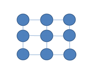
Figure 2. Separate atoms without interacting with each other.
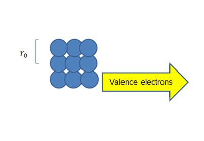
Figure 3. Atoms with real separation.
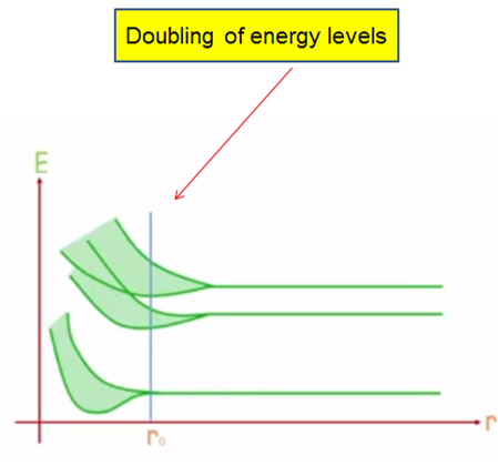
Figure 4. Diagram of how energy levels unfold.
If the number of electrons is of the order 10 ^ 24, we can consider that the energy levels form "energy bands", and between each exist and between each there are regions where energy levels are not allowed figure (5).
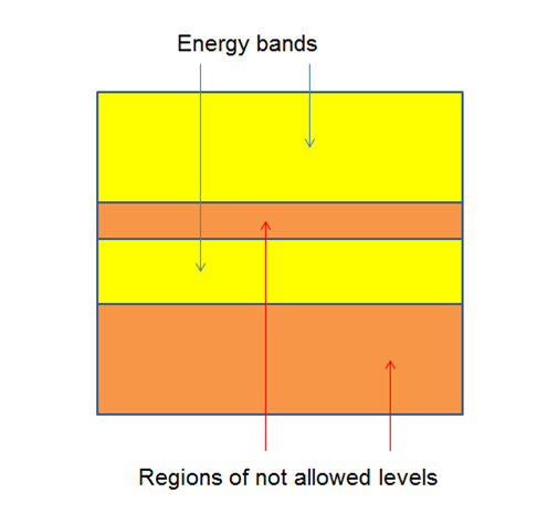
Figure 5. Energy levels.
The study of these bands allows us to determine if a material is semiconductor, conductive or insulating.
The valence band is completely filled with electrons and the conduction band is empty, by applying an electric field to the material, the electrons that were in the valence band would jump to the conduction band. In the case of semiconductors that is what interests us the band that is prohibited in the middle of the valence and conduction band, is narrower, so it is necessary to apply a less electric field for the electrons can go from the valence to the conduction, that is why the temperature increases the semiconductors increase their electrical conductivity; unlike band-band drivers is much larger and more electric field is needed for electrons to pass from one band to another.
Knowing some of the energy levels we can talk about the two semiconductor types the first:
The intrinsic semiconductor
It is very easy to identify this type of semiconductor since they are those that do not have any type of impurities, nor defects in its crystalline network, the most common or used are for example: silicon, germanium, tin. As we know if the semiconductor has a temperature of 0 degrees Kelvin, the valence band will be full of electrons and the conduction band would be empty, because there is no thermal agitation, and here we could say that the semiconductor is behaving as a good insulation. However if we increase the temperature the atoms of the crystalline network would agitate and increase their kinetic energy and this brings with it that the electrons in the valence band can absorb some neighboring atoms of other electrons inside the crystal lattice and in turn they break their bond and move through the net as free electrons, all due to their thermal agitation as I mentioned.
As they acquire kinetic energy these electrons would move to the conduction band and it is easy to analyze because if we increase more the temperature, more electrons will have in the conduction band. In this case instead of behaving as an insulator, the semiconductor acquires conductive behavior. So if an electron that is in the valence band becomes an electron this time in the conduction band, it would leave an empty position in the valence band, and if we apply an electric field, this empty position will normally be called "holle" could be occupied by another electron belonging to the valence band, which at the same time leaves another gap. This is commonly referred to as "electron-hole pairs".
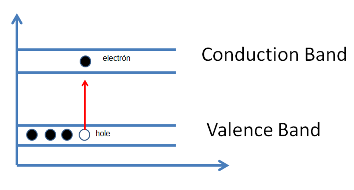
Figure 6. Thermal generation: electron-hollow pairs.
The extrinsic semiconductor
Unlike the intrinsic, these types of semiconductors are characterized by having a certain percentage of impurities, they are what we can also call as "doped semiconductors"; _ consists in the controlled introduction of impurities in the network, one element is replaced by another having an electron_; ie are those where the atoms are not even, are usually trivalent and pentavalent elements that are odd numbers. Within this type of semiconductors there are two more that are the p-type and n-type semiconductors.
Extrinsic semiconductor type p: are those that are doped with elements of the periodic table such as indium, gallium, bromine and aluminum. Since these are trivalent elements and leave a vacancy at the energy level higher than that of the valence band within its crystalline structure, there is no electron that occupies that position since they are odd elements. What causes the electrons to jump are very easily vacant, leaving free spaces or voids in the valence band.
Extrinsic semiconductor type n: are those that are doped with elements such as antimony, phosphorus and arsenic; which are pentavalent elements, that is to say that they have 5 electrons in the last layer, which means that when forming the crystalline structure, an electron is outside of any covalent link, remaining in a level superior to the other four. As a consequence of the temperature, in addition to the formation of the e-h pairs, the unbound electrons are released. The electrical conductivity of the semiconductor material would increase considerably due to this effect.
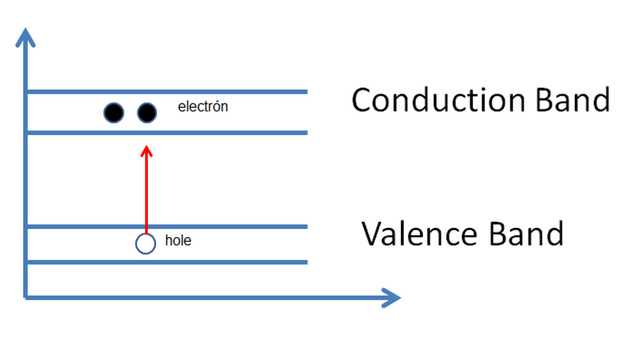
Figure 7. Effect where the electrons are the majority carriers because in the conduction band there are greater number of electrons.
"The images were made by me, if any user decides to use them in another publication should ask my permission, thanks!"
References:
- Charles Kittel. Introducción a la física del estado sólido”. Segunda edición. Editorial Reverte.
- Smith, W; Hashemi. (2006) Fundamentos de la ciencia e ingeniería de los materiales. Cuarta Edición. México. Editorial McGraw Hill.
- http://www.asifunciona.com/fisica/ke_semiconductor/ke_semiconductor_1.htm
The information is very useful for those people who are just beginning in the area of material physics, it will help them a lot.
Carlos Pagnini @carloserp2000
Physical future
Thanks for sharing I got a little bit out of it.
than you @evilmonkey
This post has received a 37.04 % upvote from @upgoater thanks to: @carloserp-2000.
All this is very interesting.
Since you put so much effort in this post I'd suggest you name your sources and credit your images with active links if you wish to gain in credibility for your posts ;)
Thank you!
the content is very good is entirely your own? ' if so, you should not mention references, but if you must take the advice to believe your images as it says @ruth-girl
thank you very much for your opinion, regarding the references do not exist because all the text was elaborated by me, and the images of the same form, but if you have reason in which I must accredit my images in some specific page that you recommend me? @ruth-girl
No references on semiconductors? Come on! This is not true. There are many everywhere! And you must heave learned that from somewhere, no?
I explain of course that there are millions of references, but I write this post with my own words of what I learned, during my studies in the area of physics I have read excellent books on the science of materials such as: Smith, W; Hashemi. (2006) Fundamentals of Materials Science and Engineering; Charles Kittel. Introduction to Solid State Physics "; William Smith. Sciences and engineering of materials, among others. Do you recommend that I mention them each time I write a paper so it corresponds to my own words and analysis? @lemouth
Well, it is a matter of giving links where interested readers can find more information on the topic you write about. That's it. Giving something readers cannot access is not really helpful. The idea is not to prove the text is yours (we have google for that), but to help your readers.
Thank you very much for your explanation and take your advice dear friend
I see dear @lemouth has explained the point of references very well!
It takes effort to create good and original (using your own words) content. I hope you'll offer that kind of posts to the platform! :D
I hope to contribute content of interest and that serves the community a lot, thank you very much for your good help
This post has received a 6.44 % upvote from @booster thanks to: @paradise-found.
Congratulations @carloserp-2000! You have completed some achievement on Steemit and have been rewarded with new badge(s) :
Click on any badge to view your own Board of Honor on SteemitBoard.
For more information about SteemitBoard, click here
If you no longer want to receive notifications, reply to this comment with the word
STOP