Learn more about the characterization of materials, "Scanning electron microscopy" technique used for semiconductor compounds Part #3
To continue talking about the SEM, in this opportunity I want to show you another detector very used for the characterization of materials in the scientific area, it is very used by us physicists, since by means of this detector we can obtain the difractograms, which at the same time In order to identify the type of crystal system to which a semiconducting compound belongs and its different phase compositions, this is very important to determine the structure of the semiconductor.
In previous posts I explained the technique of caracerization of a semiconductor by means of X-ray diffraction using the powder method; his theory, methodology and sample preparation. In this technique we use the D8 BRUKER diffractometer, these equipments are composed by an X-ray detector, which is where the electrons impinge on the sample reflecting and complying with the Bragg's law in order to obtain said diffractograms where they reflect the diffraction peaks with their respective intensities and location of angle 2Ɵ.
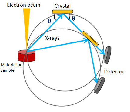
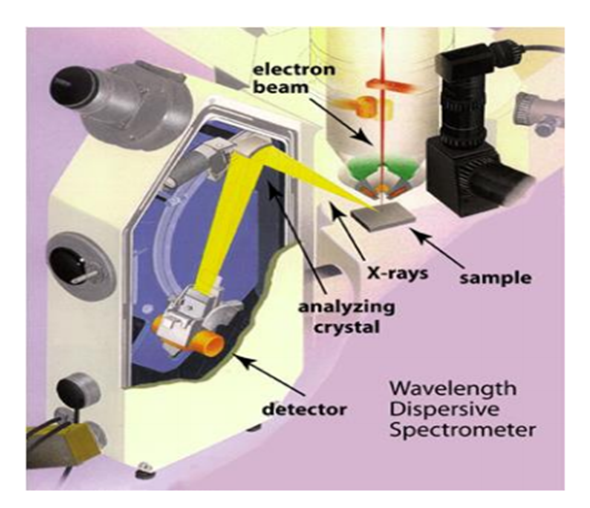
Through this detector we can analyze the X-ray spectra of any material, also measure their wavelengths. The physics used in its methodology is very simple and easy to understand, in this the X-rays emitted impact on the crystal that we want to characterize and then these X-rays are diffracted, later the X-rays arrive at the WDS detector and they give us the information of the wavelengths. The detector and crystal move on a circle of Rowland with a constant radius in order to be able to stabilize accurately at the moment of the analysis of the material, and to be able to obtain a clear and precise information of the spectrum.
The WDS is not used in all the diffractometers, since today there are other more modern detectors coupled to this equipment as the detector of scintillation. The WDS is still used for spectrometry, to determine their wavelengths, in the same way the SEM needs to study these spectra, that is why optical microscopy in my personal opinion is the best that can exist today for to be able to obtain high resolution images of any material, in science it is essential to be able to observe in detail in a microscopic way the materials that we use, because for example in the semiconductor compounds, it is necessary to be able to visualize in detail the ingot grown during the synthesis and thus be able to draw a correct analysis of the study of physical properties, that is, there are times that a compound, whether ternary or quaternary, shows unique characteristics on its surface and this happens because the elements are not synthesized in a homogeneous way and that is why at the moment of performing their respective studies of the physical properties show different results in each area of the A sample even though it is the same ingot.
WDS
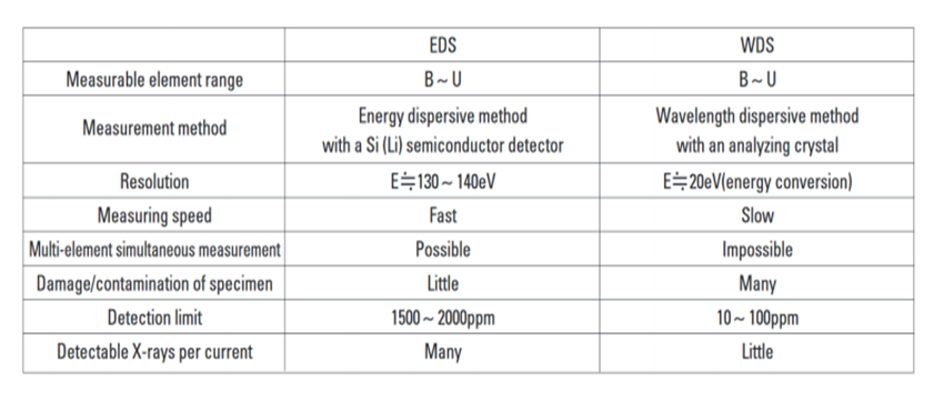
Inquiring on the web I found this interesting table that shows the differences between the EDS detector and the WDS, each one presents unique characteristics that make possible the study of different materials.
Source
In the table we can see that both use the same range to perform the sweeping of the materials to be characterized, the method they use is similar but they change their internal detectors, one has more resolution than the other and in the same way you can see that the speed and accuracy of the EDS is greater than that of the WDS, the damage of the sample in the WDS is greater because it is expected that at the end of the measurement the sample can not be used again for another type of characterization, the WDS allows trace detection Of elements. These are used in scanning electron microprobes to mainly perform elemental analysis. and finally the EDS requires a small current to be able to analyze the material and the WDS much higher.
These detectors are used for a specific purpose depends on what you want to obtain, have their advantages and disadvantages with respect to each other as for example: the WDS has to move the glass at a very precious angle so that the information can be obtained required, that is, the rays only enter by a small fraction that leave the sample, which is much more difficult when measuring. It also picks up the wavelengths very slowly with regard to the EDS which is much faster.
On the other hand it also has some advantages with respect to the EDS and is that this detector (WDS) performs a better overlap of the peaks of the diffractogram, that is, they are more defined so they do not have much noise.
Another advantage with respect to the EDS detector is that it detects very small peaks and has a better signal ratio and more accurately detects very light elements.
And finally it is easier to handle.
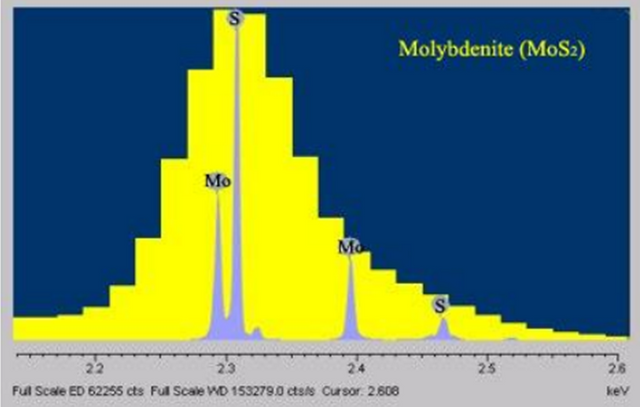
Lines of Mo and S
Comparison of the EDS vs WDS with respect to the lines of the Mo and S, as can be observed in the EDS detector these lines are superimposed, while in WDS detctor they do not present this superposition, that is, they are more defined as mentioned above.
And an advantage that both detectors have is that they can use both the scanning electron microscope (SEM) and the electronic transmission microscope (TEM).
Would you like to know more about scanning electron microscopy, then visit my previous publications:
And if you want to learn a bit about semiconductors you can also visit the following publications:
- https://steemit.com/steemstem/@carloserp-2000/do-you-know-semiconductors-your-answer-is-no-i-will-explain-to-you-very-easily-part-10
- https://steemit.com/steemstem/@carloserp-2000/do-you-know-semiconductors-your-answer-is-no-i-will-explain-to-you-very-easily-part-9
- https://steemit.com/steemstem/@carloserp-2000/do-you-know-semiconductors-your-answer-is-no-i-will-explain-to-you-very-easily-part-8
- https://steemit.com/science/@carloserp-2000/do-you-know-semiconductors-your-answer-is-no-i-will-explain-to-you-very-easily-part-7
- https://steemit.com/science/@carloserp-2000/do-you-know-semiconductors-your-answer-is-no-i-will-explain-to-you-very-easily-part-6
- https://steemit.com/science/@carloserp-2000/do-you-know-semiconductors-your-answer-is-no-i-will-explain-to-you-very-easily-part-5
- https://steemit.com/science/@carloserp-2000/do-you-know-semiconductors-your-answer-is-no-i-will-explain-to-you-very-easily-part-4
- https://steemit.com/science/@carloserp-2000/do-you-know-semiconductors-your-answer-is-no-i-will-explain-to-you-very-easily-part-3
- https://steemit.com/science/@carloserp-2000/do-you-know-semiconductors-your-answer-is-no-i-will-explain-to-you-very-easily-part-2
- https://steemit.com/science/@carloserp-2000/do-you-know-semiconductors-your-answer-is-no-i-will-explain-to-you-very-easily
References:
https://es.slideshare.net/vegabner/microscopia-electronica-de-barrido
http://www.iqcelaya.itc.mx/notasseminario071016.pdf
https://ssyf.ua.es/es/formacion/documentos/cursos-programados/2012/especifica/tecnicas-instrumentales-en-el-analisis-de-superficie/26-noviembre-tecnicas-de-analisis-quimico-superficies.pdf
Excellent post my friend @carloserp-2000. Thanks for sharing. Regards!.
Thank you friend @tsoldovieri