Learn more about the characterization of materials, "Scanning electron microscopy" technique used for semiconductor compounds Part #2
To continue the topic related to the characterization of materials, in the previous post I talked about the SEM, it is used a lot in my area to characterize the semiconductor compounds, I showed some images of photographs of the surfaces of some materials in high resolution.
In this case I will continue talking about the SEM, this microscope has the ability to perform different studies changing its detectors.
To perform studies of chemical composition of periodic table elements or any other material, we use the X-ray detector, this serves to observe the concentration of each element within the material, for example: if we have a ternary semiconductor compound, it is say, CuInTe2, we know that at the moment of making its synthesis of growth in this, a certain percentage of each element that would be 25% of Cu and In and 50% of Te was added, to obtain a total of 100% in its concentration, then for us to verify this composition we must carry out a study of chemical composition that takes by name energy of dispersive spectroscopy (EDS) or X-ray spectroscopy (EDX). Its main function is to provide an analysis by means of a diffraction pattern that shows the chemical concentration of the compound in the entire KeV range.
And then I will explain in summary way its principles of operation (this post is short I just want to show a bit of what the team is about).
It is a device that is used to characterize chemically any material. This characterization system work as a team integrated to the SEM, the EDS would be another detector type unlike the other two mentioned in the previous post that are used specifically as a photograph of the materials, in this case the EDS detector shows an analysis of greater depth of the material because it gives us information that at first sight we can not obtain. This uses the energies of the X-rays from the SEM, the interactions of the electron beam and the material.
The spectrum that originates this emission serves to identify the composition of elementary phases within the material.
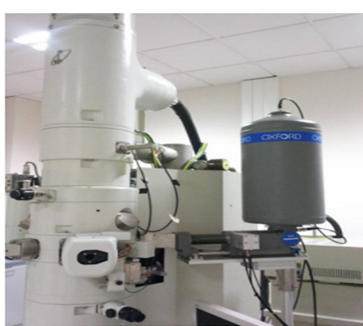
Figure 1. SEM.
Source
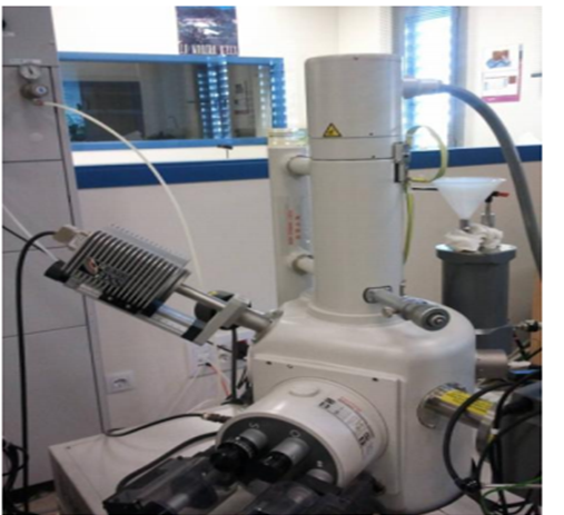
Figure 2. EDX detector.
Source
Once the samples have been placed on the SEM slide, in order to detect the signal emitted, this system is used by a silicon and lithium detector in solid state, this captures the signal of the X-rays bombarded by the SEM tube, to subsequently send a signal to an amplifier and this converts said signal and sends all the information that is collected by means of a software that determines the corresponding concentrations of the material records the data as intensity and emission energy spectra, also results in a list of each element analyzed during the sweep with each percentage of chemical concentration, atomic weight and structure examined.
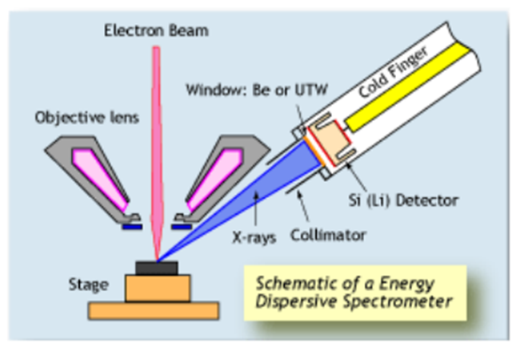
Figure 3. Scheme EDS.
Source
Electron pairs and holes are generated depending on the amount of X-ray energy entering through the window. And by measuring this signal (electrical current) the value of the X-ray energy can be determined.
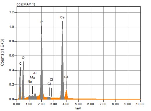
Figure 4. EDX broadcast spectrum.
Source
The figure 4 and shows a series of peaks related to the concentration of each element of the material swept by the EDS technique, the qualitative analysis in this case provides elements such as sodium, magnesium, aluminum, chlorine, phosphorus, each one is represented by a characteristic peak that reflects its intensity, at higher intensity means higher concentration and energy in KeV.
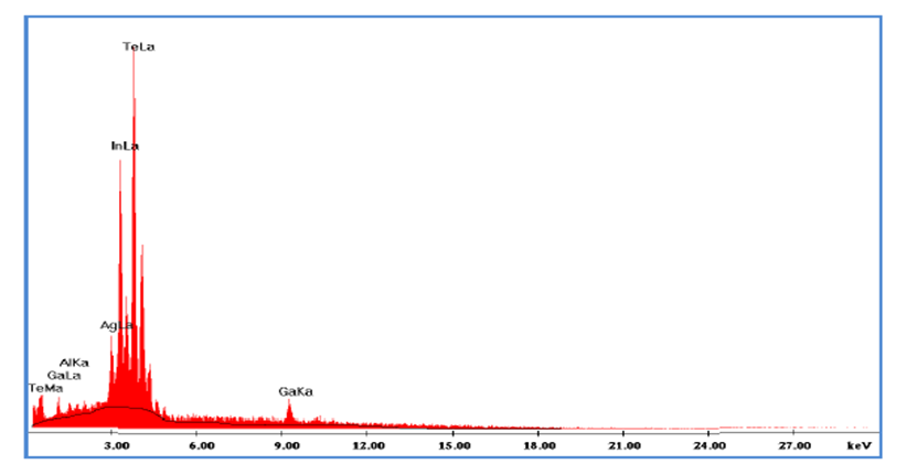
Figure 5. Spectrum of the chemical analysis of the semiconductor AgIn4GaTe8.
Figure 5 shows the EDX analysis of a semiconductor sample. As you can see, the concentration corresponds to the excess of In and Te in material, which is why the spectrum shows greater intensity in that KeV range, due to a higher percentage of these elements when making their growth synthesis.
In summary this system serves to determine the chemical concentration of the materials, important to verify if at the moment of synthesis, each element shows the concentration placed by us, see their corresponding transitions in each line of the spectrum, also observe the percentage of each element across the KeV spectrum.
References
- https://es.slideshare.net/vegabner/microscopia-electronica-de-barrido
- https://ssyf.ua.es/en/formacion/documentos/cursos-programados/2012/especifica/tecnicas-instrumentales-en-el-analisis-de-surface/26-noviembre-tecnicas-de-analisis-quimico -superficies.pdf
- http://intekgroup.com.co/servicio-de-analisis-micro-elemental-sem-eds/
- http://www.iqcelaya.itc.mx/notasseminario071016.pdf
- http://www.iqcelaya.itc.mx/notasseminario071016.pdf
- http://ri.uaemex.mx/bitstream/handle/20.500.11799/14248/403176.pdf?sequence=1
- http://tesis.ipn.mx/bitstream/handle/123456789/929/MICHELGONZALEZ.PDF?sequence=1
Beautiful Bro