Do you know semiconductors? your answer is no... "I will explain to you very easily" Part # 10
We all know what a semiconductor is and how a compound is grown, in previous posts I talked about the theoretical 1, 2 and 3part and some synthesis 2 techniques, as well as the structural characterization of these compounds.
Before entering fully into the optical and electrical characterization, first I want to show you how to prepare a small portion of the ingot grown, in order to carry out studies of the aforementioned physical properties.
The first step is of course to grow the sample, that is to say synthesize them by means of the appropriate technique for said compound.
The second step is to cut the ingot, this is done with a special diamond cutter to cut this type of materials (figure 1).
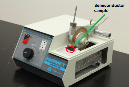
Figure 1. Special device for cutting semiconductor materials.
source
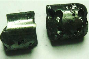
Figure 2. Ingot of a semiconductor material.
After having cut the ingot we proceed to the preparation of it (figure 2).
How to prepare a sample of a semiconductor compound to make optical and electrical measurements.
The materials to be used are the following:
Rheostat.
Plate brand BANTE MS400 MAGNETIC STIRRER.
Bee wax.
Micrometric screw.
Sandpaper.
Mop.
Process:
First the plate (figure 3) is connected in order to turn on the thermocouple (figure 4).
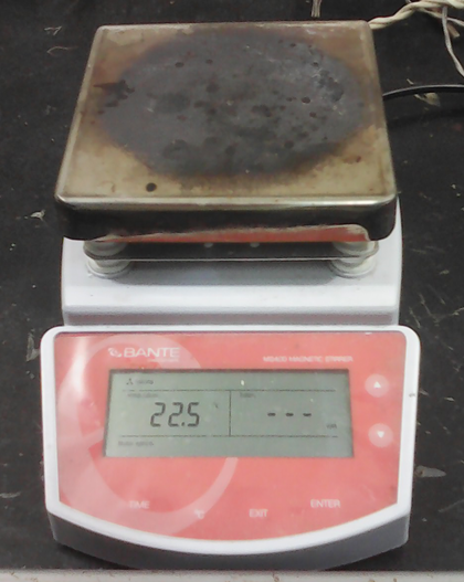
Figure 3. Plate brand BANTE MS400 MAGNETIC STIRRER.
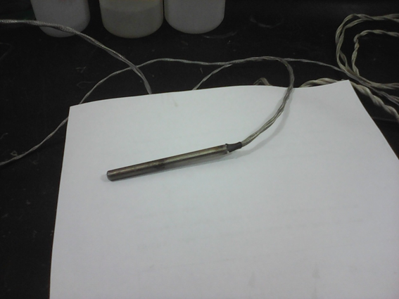
Figure 4. Thermocouple.
The iron has two connector cables, one connected to the outlet and the other connected to the rheostat.
Connect the rheostat to the power source and turn it on, placing it at 70v, and make sure that the thermocouple is on the plate. The function of the thermocouple is to verify that the temperature on the plate is correct (figure 5).
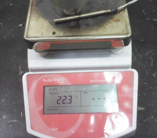
Figure 5.
Place the micrometric screw on the plate (figure 6) and wait for it to warm up to a temperature of approximately 80 ºC.
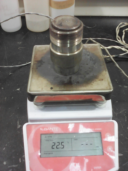
Figure 6.
Allow 10 minutes for the screw to acquire the desired temperature, then place the beeswax and wait until it melts a little and place the sample of the semiconductor material on the screw (figure 7).
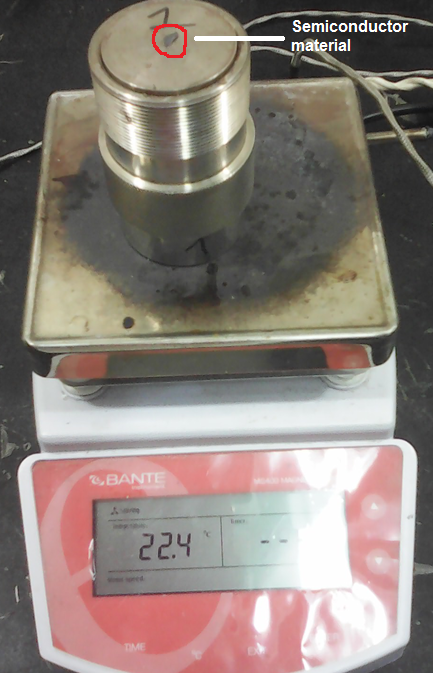
Figure 7.
The wax can not be appreciated because at the moment of melting it adheres to the screw next to the sample and its tone is transparent.
Remove the screw from the plate and wait for it to cool, so that the wax hardens and keeps the sample fixed on the screw (figure 8).
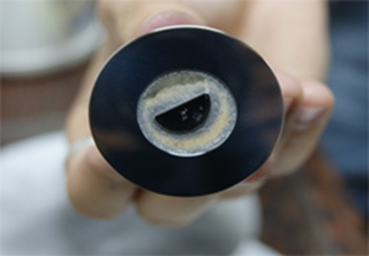
Figure 8.
Source
With the screw we measure the thickness of the sample, in such a way to have the precise measurement of the thickness of the sample to later reduce its thickness.
Then proceed to reduce the sample with a sandpaper of (400 / PB800) (Figure 9) to reach the thickness required by us, remember that the micrometric screw is given in microns. The sample will be manually reduced by turning the screw in the shape of 8 (figure 10), this technique is done so that the sample is flat on its surface.
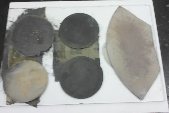
Figure 9.
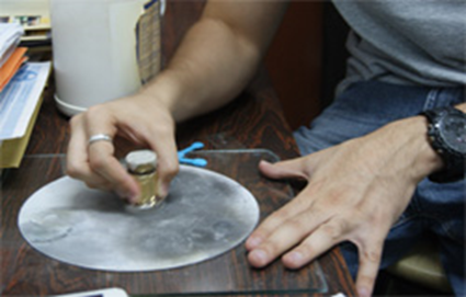
Figure 10.
Source
Finally, proceed to polish the sample with a gray mop of 0.05μm and 0.3μm (figure 11), so that it is bright on its surface, without impurities or any other defect, so that at the time of completion optical and electrical measurements the margin of error is not significant.
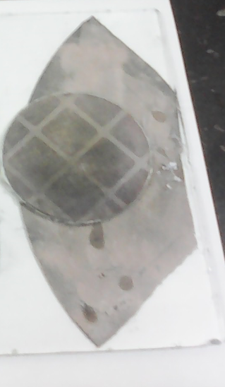
Figure 11.
And perform the same procedure for the other side. We must turn the iron on again, place the screw on it and wait for the wax to melt so that we can remove the sample and do the procedure on the other side, just as I explained it. To clean the sample we must use chloroform or isopropyl alcohol, in a biker or any glass container we fill it with liquid and place the sample for about 5 hours so that it will take off all the wax and so we can make the measurements.
And that's all.
It should be remembered that for optical measurements the sample of the material must have a thickness of approximately 50microns, that is, have the thickness of a sheet of paper and both sides are very polished that we can reflect on the sample: D.
And for electrical measurements the thickness is not so small, it is recommended to have a thickness greater than 300microns but if both sides and sides are polished.
Later on I will show you the experimental setup to characterize semiconductors through optical and electrical measurements.
References
- http://www.bante-china.com/enproductsview/807.html
- https://en.wikipedia.org/wiki/Thermocouple
- http://www.physics-and-radio-electronics.com/electronic-devices-and-circuits/passive-components/resistors/rheostat.html