Do you know semiconductors? your answer is no... "I will explain to you very easily" Part # 7
As they are friends of steemit, I disappeared a few days because I am very busy with my thesis of undergraduate, I have advanced a lot with respect to my work and it lacks little to culminate.
To return to the topic of semiconductors in this opportunity I want to advance a little more, I showed them at the beginning the basic concepts of semiconductors, all the theory necessary to understand these materials that have many applications in modern technology, of some techniques to grow this type of compound and to convert several elements into one by means of a kind of "stone" or "ingot" to call it that way.
But you ask yourself: what can be done after obtaining these ingots? This answer will clarify as you write different publications, which would be the different techniques of characterization of these semiconductor compounds.
These characterization techniques are extremely important because it is there that we will physically study the different properties of these compounds, then have adequate information and analyze them so that they can serve, that is, what application they can have at present and in the future.
The following is a brief summary of some of the techniques for structurally characterizing a semiconductor compound, which is used in the Laboratory of Structure and Engineering of Nanostructured Materials.

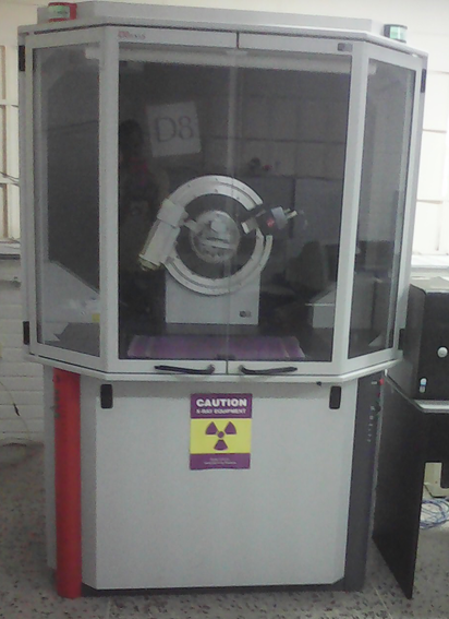
Figure 1: D8 Focus-Bruker Diffractometer.
When we speak of structures in a semiconductor we speak of crystalline systems, in a post previously explain what these crystalline systems are and how they are shaped.
Each semiconductor compound corresponds to a crystalline system, which in turn is formed by the ordering of atoms in that system either tetragonal, hexagonal, triclinic, and so on. In my case the compound that I am studying in my undergraduate thesis presents a "tetragonal" crystalline system that is the CuInTe2, and the question is how we determine that crystalline system, it turns out that to reach that step we first need to characterize the semiconductor by medium of a technique and is as follows:
Earlier I also spoke a bit about x-ray diffraction and the bragg law, to remember I would say that diffraction is a wave phenomenon, that is, it leads to the generation of constructive and destructive interference between waves that are dispersed by a medium material.
When we characterize a semiconductor by means of a specialized apparatus for this technique, in which an electron beam is impinged on the atoms of a material, these electrons vibrate harmonically at the frequency of the incident radiation undergoing an acceleration (1).
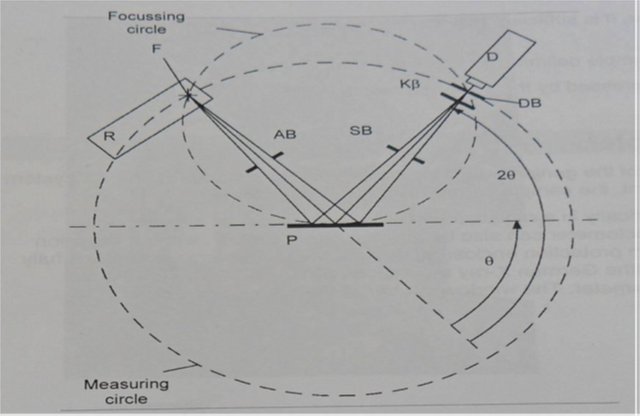
The interatomic distances in the crystals are of the order of 1 Å. The electromagnetic radiation whose wavelength is 1 Å corresponds to the X-rays, therefore, the crystals act as X-ray diffraction gratings. This fact constitutes the basis for the determination of the crystal structures. Bragg gave an explanation to the diffracted beams observed when a monochromatic light strikes a crystal. If λ is the wavelength of the radiation used, dhkl is the distance between planes of indices hkl and in addition λ ≤ 2dhkl then: 2dhklsenθ = n λ n = 1,2,3.
Where: n: 0, 1, 2, 3, ...... .ny corresponds to the order of the dispersion, θ: is the angle at which the maximum diffraction or Bragg angle appears and can be chosen simply by rotating the crystal to x-rays. The wavelength (λ) of the incident radiation has a fixed value, dhkl is the distance between families of crystallographic planes, which have a fixed value determined by the cell size and the Miller indices, which indicate the direction of the planes inside the glass (2).

Figure 2. X-ray incidence scheme in the diffractometer sample (3).
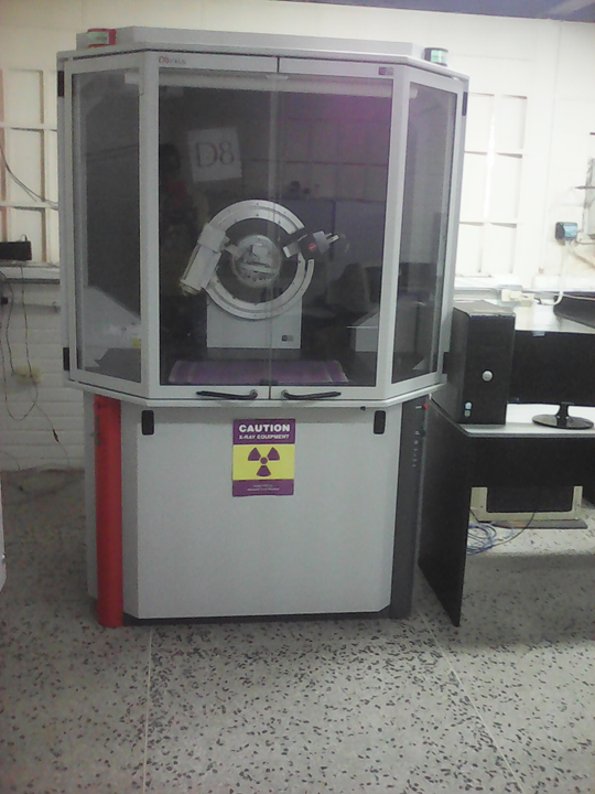
Now for us to characterize these semiconductor compounds we use a Focus-Bruker D8 diffractometer (figure 3), which has a goniometer that has an X-ray tube placed at one side, which in turn causes an electron beam to strike the center of the sample is then diffracted to be captured by a Lynxeye linear detector, the angle being equal to the diffracted angle. The head of the goniometer moves circularly at an angle of 2θ, and then the apparatus performs the recording of intensities as a function of the angle, by means of which the "bragg law" will be fulfilled.

Figure 3. Diffractometer used in (LEMIN) for the structural characterization of semiconductors.
It must be taken into account that for us to place the sample of the semiconductor compound inside the sample holder of the diffractometer, we must previously crush it and turn it into powder, which is why the name is given to this technique.
This X-ray diffraction equipment is characterized by great accuracy and versatility of use. It is equipped with an X-ray source with copper anode, high stability, uses a scintillation detector and a linear one.
After performing the scan of the sample through a computer program that comes with the equipment, this as I told you record the sample intensities of the compounds as a function of the angle, after obtaining this record, the file we can see by means of computer programs either: SEARCH-MATCH, FULLPROF, among others.
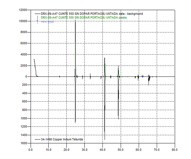
And it will show us a diffraction pattern of this type (figure 4):

Figure 4. Pattern of diffraction of a semiconductor.
The figure shows two patterns of diffraction in the upper part of the sample of CuInTe2 semiconductor, which is the sample that I am analyzing in my undergraduate thesis, and in the bottom is shown another pattern of diffraction that is also the material CuInTe2 , but unlike this material is already registered in the database of the SERACH-MATCH computer program, that is to say my sample does not yet present publications in any scientific journal, instead the other material if and in the graphic you can see the report number in the program database (34-1498).
And you wonder why I compare my material with another, I do this in order to see if in my compound the phases of the material are the same or are in the same range as another already reported, ie in the X axis (2θ ), the Y axis presents the register of the intensities in each phase of the material. In some the intensity is higher because there is greater concentration of the semiconductor element in this location.
Well for the moment I will leave the post here, I will post the continuation where I will explain in detail what each graph means and why I perform this analysis and for what it serves me.
I hope you liked my publication and be of your liking, if you have any doubts about it do not forget to leave your comments and I will gladly clarify those doubts.
References:
(1) Heredia, K. (2014). Structural, optical and electrical characterization of the semiconductor AgIn5Te8 to be used as absorbent material in solar cell prototypes. Thesis presented in option to the academic title of master in Science and Technology of the Materials. Cabimas. University of Havana, Institute of Science and Technology of Havana, pages 39 and 40.
(2) Henry, Lipson and Wooster, Interpretation of X-ray Diffraction Photographs (Longmans Canada Ltd, Ontario, 1960).
(3) Loaiza, A. (2014). Synthesis and physical chemical characterization of the semiconductor AgIn5,01Te8 .. Thesis presented in option to the academic title of master in Science and Technology of the Materials. Cabimas. University of Havana, Institute of Science and Technology of Havana, page 32.
Hay que hacer varias precisiones al respecto de su post. ¿Qué sucede cundo no cuenta con suficiente muestra del semiconductor que ha sintetizado y no alcanza para llenar el portamuestra de llenado frontal? El equipo que muestras en las imágenes es un difractómetro modelo D8 Focus, marca Bruker y serial 203420 que posee un detector Lynxeye y no de centelleo. Los datos son colectados y con ayuda del paquete informático Eva que hace parte del equipo y que posee la aplicación Eva-Search Match se realiza el análisis cualitativo, una cosa importante el programa debe tener compilada la base de datos de difracción PDF-2, porque sin ella no puedes realizar la búsqueda y comparación. Otro programa con el cual puedes realizar cualitativo es el paquete de Crystallography. Los dos programas son de usos comercial, es decir, hay que pagar unos cuantos miles de dólares por ellos. No, se si el programa de uso libre, Fullprof tenga compilada la base PDF-2. Bueno amigo @carloserp-2000 muy bien por el esfuerzo de explicar la técnica de difracción de rayos X para caracterizar cualitativamente semiconductores. Saludos
Many thanks for the comment and add your suggestions, I guess you are a great connoisseur of the structural characterization technique of semiconductors
Later on I will speak more about the program for the qualitative analysis in this opportunity only to show the team with which the diffraction patterns are obtained
This post was resteemed by @steemitrobot!
Good Luck!
The @steemitrobot users are a small but growing community.
Check out the other resteemed posts in steemitrobot's feed.
Some of them are truly great. Please upvote this comment for helping me grow.