Electron backscattering diffraction (EBSD) / technique used in the scanning and transmission microscope
Following the same line of research that I have been explaining in my previous publications (see the end of the post), this time I will give a brief summary of another technique of structural characterization of materials called "diffraction of electrons by backscatter" that in their Acronym is known as (EBSD).
Unlike with the previous techniques, it has the possibility of adapting to both TEM and SEM, and is used in the same way to study all aspects related to mono and polycrystalline materials, basically it is very similar to the techniques mentioned above (see at the end of the post).
It is used specifically in the crystallography of materials to determine phases, orientation, size and location of atoms within the crystalline structure.
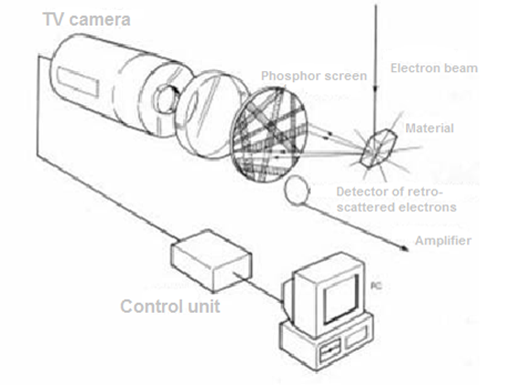
The configuration of this characterization equipment detects and analyzes the beam of retro-projected electrons, they provide all the necessary information after the electrons impact on the sample, to then make their respective analysis of the diffractogram.
The adaptation of the scanning and transmission electron microscope allows to combine this technique (EBSD), by means of the detectors of secondary electrons or retridispersed electrons, and this is the great difference that it has with the other characterization techniques. It is a great advantage that It allows to use any of the two detectors.

Source
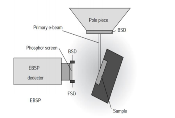
Basically the sample of poly or monocrystalline material that is desired to characterize is incorporated, inside the microscope chamber either of scanning or of transmission, then this chamber is oriented towards the detector placed with an angle between 70 and 80º with respect to the tube where the electrons that must influence the sample are bombarded, in order to decrease the power of the electrons travel that absorbs the material.

Scheme of EBSD through the SEM
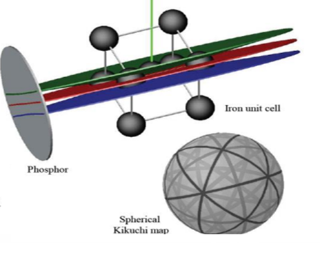
For this purpose we can analyze more easily the diffraction phenomenon that occurs through the retroprojected electrons, which for this reason receives the name of this technique. These electrons leave the surface of the sample and are reflected in a phosphor screen placed at the end in a camera that records the data and show a diffractogram where the diffraction patterns are usually displayed, in this technique called Kikuchi patterns.

Kikuchi lines produced by diffraction of backscattered electrons.
Kikuchi lines pair up to form bands in electron diffraction from single crystal specimens, there to serve as "roads in orientation-space" for microscopists not certain at what they are looking. In transmission electron microscopes, they are easily seen in diffraction from regions of the specimen thick enough for multiple scattering. Unlike diffraction spots, which blink on and off as one tilts the crystal, Kikuchi bands mark orientation space with well-defined intersections (called zones or poles) as well as paths connecting one intersection to the next.

lines of Kikuchi.
Wikipedia

EBDS configuration by TEM
Through TEM or SEM we can obtain the following information:
Identification of crystalline phases in materials.
Texture of the material.
Alignment of atoms within the crystalline network of the material.
Grain size.
Interplanar distance.
Formations and malformations within the crystalline network.
In my personal opinion, the great advantage of this technique is that by means of its detectors, both secondary and backscattered electrons can be easily accommodated with scanning and transmission microscopes, so this technique is basically characterized by its versatility.
This technique is little used in the area of materials science since it does not have as high resolution as the EDS or WDS detectors, both can similarly identify phases and other studies on the crystal network and in addition to see surface materials.
In the next post I will write about the preparation of samples in this technique and the HOUGH transform.
Thank you very much for your attention.
If you want to see more about electron microscopy visit my previous publications:
And if you want to learn a bit about semiconductors you can also visit the following publications:
References:
Since no one else commented I thought I might stop by and say hello. You do interesting work! Do you know how deep below the surface of a material can you reach with EBSD?
Hello @aboutcoolscience thank you very much for reading my publication and commenting and clarifying your doubt this technique only makes it possible to characterize the surface of the material, so that diffraction patterns and kikuchi lines can be observed correctly. Your preparation must be very careful and correct because Some deformation in its layer can cause unwanted results.
To conclude the technique only records data of its surface, the electron beam can not reach more depth, changing the detector by an EDS or WDS if it could obtain data from the inside of the material.
I hope my answer has served you friend: D
thanks! so do you have to sputter-coat the samples before characterizing them?
Not only have to clean and polish them well so that there are no defects in their surface that can damage the measurement for example corrosion, in my next post I will explain the method of preparation I hope you like it
sure, thanks