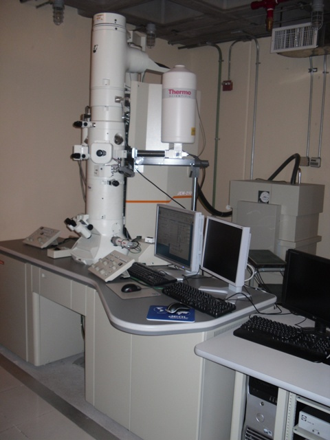
Transmission electron microscopy (TEM) another technique used in the characterization of materials
Hi friends, to continue my explanation of the different techniques of structural characterization, today I want to talk about another device used in this type of analysis, which is the transmission electron microscope (TEM), used in the same way as the SEM, both specialized in the structural characterization of materials, in my case semiconductor compounds, the application of TEM is basically the same as that of the SEM, but it has its small differences and then I will show what this electronic microscope is about.
TEM
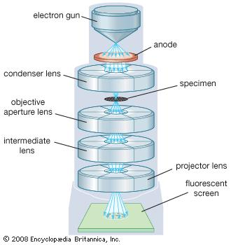
This microscope is responsible for emitting a beam of electrons, this is directed towards the material you want to observe. A portion of the electrons bounce off the material and the other part is absorbed by the material and in this way the image that the microscope increases is formed. The electrons have a much shorter wavelength than visible light and the SEM, so they show smaller structures.
The images that are increased in the TEM offer important information about the structure of the material and how the TEM can also be seen its surface, in this case we can corroborate if the material is amorphous or crystalline.
If the material presents a cirstaline structure, in this the condition of Bragg can be fulfilled and the electrons are coherently diffraten the incident electronic wave. So it is expected then that we have a diffraction diagram, which does not give valuable information about the structure and orientation of the transmitted and deviated electrons.
Like the electronic transmission microscroscope in ETSE, it is possible to study the chemical composition of a material, that is, what percentage of elements are inside it, and also a complete crystallographic study.
source
- ** Electron emitter:**
From which a narrow beam of electrons is generated. The high-energy electron beam can be obtained in several ways:
By thermionic emission.
By field emission.
Optical system:
An electron beam increased and focused either by electric or electromagnetic lenses is used. For many years scientists have studied and observed which of the two types of lenses is of better quality and concluded that the magnetic lens is better due to its precision at the time of observing the material. Then said lens has the specific function of creating fields that direct and focus the electrons, since it has the advantage with respect to optical microscopes that these do not work with electrons.
- Condenser:
By including a capacitor in this system we have the facility to obtain higher resolution images, since this capacitor conformed by an electromagnetic lens, the electron beam can be focused more precisely on the material.
- Platen:
In this devices, the plate is placed in the copper covered grille, in which the sample of the material has been mounted. The plate must be kept very clean, otherwise the movement of the sample will be affected, obstructing the observation.
- Vacuum system:
It is very important that in this tube the collision of the electrons with the molecules of the air is not found and these can be correctly diverted in the vacuum.
That is why the electron beam used in electron microscopy must travel in a vacuum space, that is, well evacuated and without air molecules. The air pressure in the microscope column should be between 10-4 to 10-5 mm Hg. This is considered as high vacuum and is produced by the use of mechanical pumps that extract air from the interior of the microscope column.
Without a doubt, it is the fundamental part for the correct operation of the microscope and it is possible to visualize high resolution images.
- Screen or viewfinder and the camera:
It is the final part of the measurement, where we can visualize the material characterized, in this case the image is projected on a screen in which the energy of the electrons is transformed into light thanks to the physics used in this case such as fluorescence.
Finally we can observe in high resolution and very close to the material, it should be remembered that this microscope can bring the material up to my times.
The images can be recorded on a photographic film. Like the photons, the electrons to influence the photographic emulsion produce changes in the silver bromide crystals, obtaining a negative in black and white, which once revealed by classical photographic methods can be copied on paper. In this way, the microphotograph (micrograph) is obtained electronically.
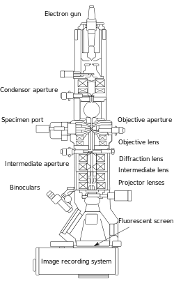
Composition / parts of TEM
After explaining the parts of the TEM, it is also important to learn how to prepare the sample to be characterized.
To use this equipment it is necessary to prepare the sample of the material, whether semiconductor or other, in the form of an ultra-thin or thin sheet, it is usually cut into a disk with an approximate diameter of 3 to 4 mm, the sample must be sufficiently fine so that the electrons penetrate through the sample and the image can be obtained in the way we want.
The thickness of the sample varies depending on the material we are going to characterize, a thickness of about 100 microns is commonly used for elements with a high atomic number, which offer greater resistance than those with a lower atomic number, usually then it varies between 100 and 200 microns.
One of the main sample preparation techniques that are used for the characterization by means of the transmission electron microscope is the mechanical and frosted cutting that consists basically of the elimination of material using abrasive particles in the successive refinement steps, in order to eliminate the material of the surface until achieving the required result.
The grinding consists of the elimination of all the defects of the material, corrosion, rust, deformations so that it is completely flat for a better analysis and obtain results.
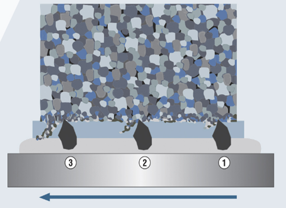
Mechanical cutting and frosting
Electrolytic polishing is used to thin the material correctly without errors or imperfections in its surface, in this process all roughness of the material is removed, leaving it free of dirt.
Electropolishing is a surface treatment by which the metal to be polished acts as an anode in an electrolytic cell, dissolving. With the application of current, a polarized film is formed on the metal surface under treatment, allowing metal ions to diffuse through said film. cited text
Electrolytic polishing
Ionic engraving (used with insulating materials and metals).
Ionic engraving
It is crucial that any damage to the layers produced in the preliminary mechanical preparation is completely eliminated in the successive steps of electropolishing or ion etching. The final thinning continues until the first hole appears next to the center of the disc; Then, the electropolishing or ion-etching processes stop immediately. The thinner parts adjacent to the hole are often thin and transparent to the electrons. If the electropolishing or ion etching is continued, the thin and transparent sections to electrons adjacent to the hole will be removed and the remaining material may not be thin enough to allow the electron beam to enter. source
The transmission electron microscopy has different applications and serve to study practically the same as the SEM, in this case all kinds of materials, but we must take into account different factors or measures of care when measuring, that is, their results depend largely on a correct preparation of a sample, its proper dimensions and its different ways of preparing as explained above. Due to its characteristics, it is an important tool for the structural characterization of nanostructured materials, from which it is possible to obtain not only morphological information, but also crystallographic and chemical composition with the help of the detectors, among them the EDS.
For more information visit the following links.
https://en.wikipedia.org/wiki/Transmission_electron_microscopy
http://www.upv.es/entidades/SME/info/753329normalc.html
https://es.slideshare.net/andi_lake/microscopia-electronica-de-transmision
http://www.cciqs.uaemex.mx/index.php?option=com_content&view=article&id=80&Itemid=82
http://www.medic.ula.ve/histologia/anexos/microscopweb/MONOWEB/capitulo5_2.htm
http://www.struers.com/es-ES/Knowledge/Special-applications/Transmission-Electron-Microscopy#tem-how-to
http://www.thierry-corp.com/mx/plasma/aplicaciones/grabado-ionico-reactivo
If you are curious to learn a little about electron microscopy visit my previous publications:
Congratulations @carloserp-2000! You have completed some achievement on Steemit and have been rewarded with new badge(s) :
Click on any badge to view your own Board of Honor on SteemitBoard.
For more information about SteemitBoard, click here
If you no longer want to receive notifications, reply to this comment with the word
STOPThank you @steemitboard
Real university grade text. We have recently got very nice scientific toy, called the Nano Tweezers, you will probably like it: https://steemit.com/science/@alexs1320/stretching-the-dna-by-nano-tweezers-so-cool