Semiconductor Physics: Part 7 - Manufacture
In the last post, we discussed a wide variety of phenomena related to strain, concluding by introducing the notion of self organised quantum dot growth via island formation, as a result of the growth of two materials with very different lattice constants at a heterojunction. In this post, we will introduce the metal organic chemical vapour deposition (MOCVD) growth process, as well as reviewing a 'top down' method of fabrication, before shifting our attention to the notion of a cleanroom, and why it is necessary.

MOCVD
Metal organic chemical vapour deposition, or if you read the Russian papers; metal organic vapour phase epitaxy (MOVPE), is a process that facilitates the growth of single or polycrystalline thin films. In this process, some really quite horrible gases, such as indium phosphide, are injected into the reaction chamber and undergo a series of chemical reactions. At the surface, cracking occurs, leaving behind the desired chemical, with the waste material being pumped away. This leads to the deposition of layers of chemical on the surface, and is in fact an equilibrium, or continous process.
A typical example of such a sample growth process might begin with a compound such as tri-methyl-gallium and arseine (not nice), with the reaction taking place at 700 deg C under hydrogen. It is quite possible to build up eptaxy and different materials by switching between different gases.
MOCVD is a much quicker process than MBE since the pressure of the gas can be really ramped up quite a bit, with epitaxy every bit as good as MBE, at five times the rate of production. This makes MOCVD a great choice for industrial application.
One slight quirk with MOCVD - groups worldwide are growing rods/pillars by introducing Au nanoparticles to a surface, leading to preferential growth under the Au catalytic seed, thence the formation of pillars. It is possible to grow tremedously good 1D III-V nanowires under such Au seeds. However, much like Stranski–Krastanov QD growth, the process is random and self assembled.

II-IV mateials such as CdTe, CdSe, etc. facilitate the formation of quantum dots, chemically via small inclusion of semiconductor in chemical techniques, such as coagulation. You can buy QDs of different sizes, where the size is related to the emission wavelength. From an engineering perspective, these are pretty useless but have been put to good use in medical diagnoistics as biomarkers. The materials involved, however are pretty nasty, you wouldn't want them in your body for very long (or at all!).
'Top Down' Example
We have been looking, so far, at bottom up processes that take atoms and make them into nanostructures, atom by atom. Now we are going to think about taking something big and, effecively chopping it up.
If we start with nice, thin MBE grown sheet, put some metal on the top and put a volage through it, the electrons udnerneath the metal will be excluded. This works in the same way as a field effect transistor. All electrons under metal are repelled and excluded, and it is possible to make this region into a single electron island: playing around with surface gates, it is possible to constrict a sheet of charge into smaller dimensional regions. It is possible to make just a wire, or a complete dot. This method makes possible the construction of many different nanostructure designs in a rigorous, well defined manner.
What is a cleanroom?
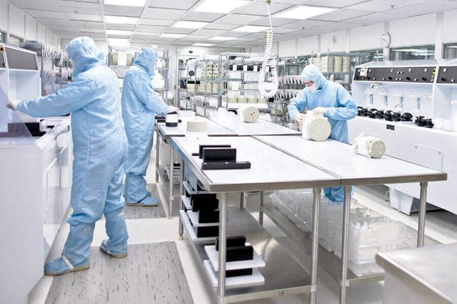
Aside from being clean in the conventional sense, the main aspects of a cleanroom are that the temperature and humidity are controlled. Invariably, in a cleanroom you want to be able to do the same thing twice. This is important for industry, as you don't want bits of your circuits knocked out by contaminants! On the other hand, in research, it's not terribly important if this happens to a few of our circuits, we will just throw them away and make some more.
Humans in a cleanroom are the biggest problem, with hair being the biggest source of dust. It is necessary to wear gloves and a suit while in the cleanroom so that dust from your head falls into your suit and into your shoes so that you take the dust with you out of the door, when you leave. Large scale industrials nanofabrication labs usually do away with people, apart from when things need to be fixed! A class X clean room has X identifiable particles above 0.5 micrometers size per meter cubed.
In the next post, we will lock in our attention on fabrication methods, with particular focus on lithography.
This post has been ranked within the top 25 most undervalued posts in the second half of Apr 29. We estimate that this post is undervalued by $7.25 as compared to a scenario in which every voter had an equal say.
See the full rankings and details in The Daily Tribune: Apr 29 - Part II. You can also read about some of our methodology, data analysis and technical details in our initial post.
If you are the author and would prefer not to receive these comments, simply reply "Stop" to this comment.