Semiconductor Physics: Part 5 - Manufacture
In the last post, we considered step flow growth, reflection high energy electron diffraction (RHEED), and studied MBE through the lens of the gas laws, predicting the length of time it takes for a clean surface to become contaiminated. In this post we will take a deeper look at binary and tertiary semiconductor heterostructures through the lens of the bandgap.
Bandgap vs. Lattice Constant for Typical Semiconductors
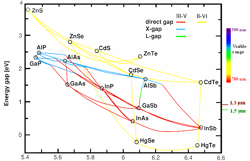
The figure below presents the bandgap vs. lattice constant for the majority of popular semiconductors. The colour scale roughly characterises the energy at which a photon would be emitted at the bandgap. The joining of the lines is intended to provide insight into alloy properties. It should be noted, however, that the reason behind the bowing is not yet understood, in full; the figure was generated with empirical fits.

Direct/Indirect Bandgap Materials
In direct bandgap materials such as GaAs, InP, InAs, InSb, GaSb, the zone centre of the E(k) dispersion has its minimum energy for the electron at the same wavevecor as the maximum energy for the hole. This means you get roughly parabolic dispersion which coincide at the same point for their minimum and maximum. All these materials exmit light strongly. This is not the case for semiconductors such as Si, for example, which are characterised as indirect bandgap materials. In these semiconductors, the zone centre isn't the location of minimum energy that the electron can inhabit.
Vegard's Law
Vegard's law formalises the linear interpolation between two binary materials, generating a first approximation of lattice parameter, and therefore broadly the bandgap, however notable exceptions exist for this rule. For example, if we consider a straight line drawn between InP and InAs in the figure, we see that as we 'take out' some of the As, and 'add in' P, according to

the bandgap roughly evolves as

Terms can be added to this simple interpolation in order to attempt to model the non-linearity of the joining on the interval under consideration. This is referred to as a bowing parameter. As can be seen in the figure, the bowing parameter can vary drastically on different intervals.
Anderson's Rule
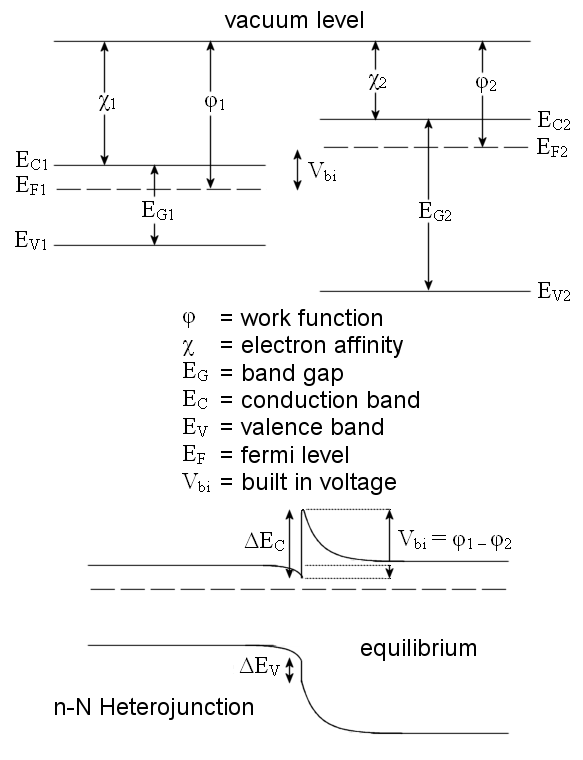
Anderson's rule helps us to determine the relative alignment of the bandgaps when two materials are grown at a heterojunction. It is the case, however, that Anderson's rule works for only 80-90% of the III-V semiconductors. The most common expection is GaAs/AlGaAs.
Anderson's rule states that the difference in the conduction band edges at the heterojunction is equal to the difference in the electron affinity (the energy you need to take an electron from the conduction band to the vacuum level) of each material.

In a scenario where you have a smaller bandgap sitting completely within the wider bandgap, you have a type I heterostructure. If there is a negative offset in the valence band, and the bands are misaligned, you have a type II heterstructure. In the extreme case, where the difference in the electron affinities is greater than the one of the bandgaps of the material, you have a type III heterostructure, where the materials are aligning with a complete mismatch of bandgaps.
