Semiconductor Physics: Part 4 - Manufacture
In the last post, we introduced the top down and bottom up regimes of semiconductor manufacture, as well as the process of molecular beam epitaxy (MBE), and the notion of a substrate. In this post, we will continue with these themes, extending to step flow growth, reflection high energy electron diffraction (RHEED), and we will further consider MBE through the lens of the gas laws.
What Happens at the Surface?
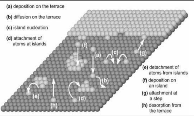
There are many processes that can occur at the surface. These include:
- Deposition on the terrace: the atom can approach an isotropic plate plane and stick to the surface.
- Diffusion on the terrace: with enough energy, the atom can wander around on the surface. This is actually quite a desireable scenario.
- Island nucleation: clusters of atoms, which have started to find their minimum energy position within the lattice.
- Attachment/detachment from islands: the danger is that the flat, one-atom thick layer can be lost through pyramidal formation through the attachment of atoms to the top of islands.
- Step flow growth: described later.
Reflection High Energy Electron Diffraction (RHEED)
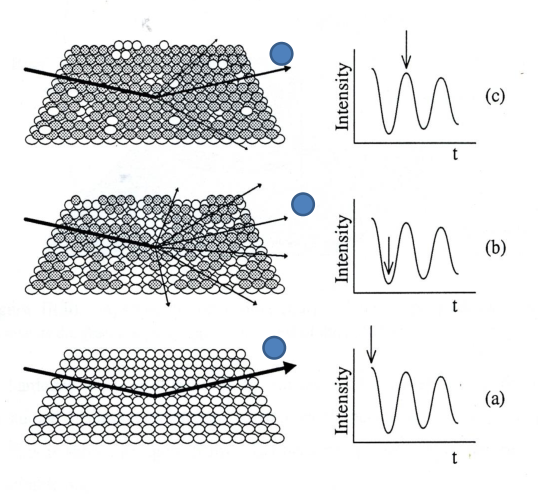
If we have a grazing incident angle of electrons hitting an atomically clean surface, then the angle of reflection and incidence are equal, and you get a high intensity at this angle. But then, as the growth process begins, a random arrangement of atoms on the surface develops, leading to specular reflection as a result, and the intensity drops.
Eventually, we have enough material on the surface so that we have an almost clean atomic layer, and the intensity increases once again. The RHEED oscillation has a decaying envelope due to the imperfection of the surface: as the envelope decays, the 2D growth gets worse and worse - tending towards a 3D structure. It is the case that every RHEED oscillation corresponds to an atomic layer, so you can quite easily count the layers by looking at the intensity graph. The grower uses these RHEED oscillations to calibrate the rate of growth for given cell temperatures.
Step Flow Growth
We can artificially engineer substrates that have a slight mis-cut, so we actually have step terraces. When we grow with step terraces, defects are minimised since the energy of the atoms on the lattice is minimised at terrace steps, resulting in much better 2D growth - the interface roughness is a lot better.
MBE Machine & Gas Laws
A flux of molecules incident upon a surface is given by
where n is the number density of molecules, and v is the mean velocity. Now, pressure, temperature and volume are related via simple gas laws
The average velocity is related to the thermal energy by
where we have
which leads us to
The combination of these results yields
How Clean Can We Keep a Surface?
We calculate a background flux, assuming that hydrogen comprises the majority of the species. In a typical MBE mahcine, we have a pressure of ~5x10^-9 Pa, a number density of molecules ~1.2x10^12 per m^3 which leads us to a background flux of ~5.4x10^14 m^-2 s^-1.
Now, we need to know the density of atoms in a monolayer of contaminant. If we assume that bonding takes place at surface atoms only, and suppose we have a GaAs lattice, which has two atoms per unit cell (100 orientation), then the density of atoms in each monolayer is
Now, by assuming that the 'sticking coefficient', zeta =1, we can predict the amount of time the surface will remain clean as
which is roughly 3 hours!
In the next post, we will consider binary and tertiary semiconductor heterostructures through the lens of the bandgap.


