Semiconductor Physics: Part 3 - Manufacture
In the last two (i, ii) posts, we discussed nanostructures and confinement regimes. In this post, we will begin to explore the ways in which low dimensional semiconductor devices are made, or grown.
Terminology
Top Down
In 'top down' approach, you start with some macroscropic structure, and proceed to make it smaller. This approach is often extremely expensive, requiring large scale facilities.
Bottom Up
In the 'bottom up' approach, you start with atoms, and assemble them in some way to create nanostructures. Often this process is random and dominated by self-assembly mechanisms, being extremely difficult to control.
Molecular Beam Epitaxy
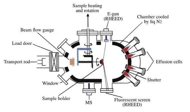
One such example of a bottom up process is Molecular Beam Epitaxy (MBE). This method was pioneered in the late 60s and early 70s, and made possible the contruction of structures one atom in thickness. In general, the process is characterised by the elemental decomposition of materials in ultra-high vacuum (UHV) and is an outstanding growth process for quantum wires and quantum dots. The general schematic of the MBE machine is shown in the figure below.

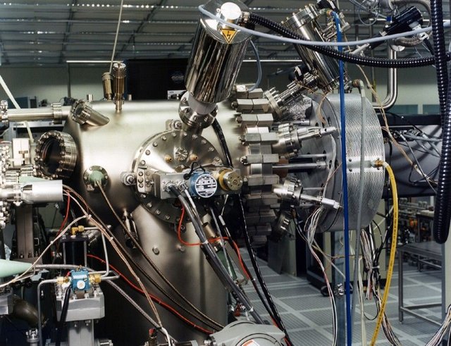
The MBE machine is a vacuum chamber, which facilitates the heating of metals in order to generate vapour. There are a series of shutters that block/unblock the beam of vapour coming off the cells. The critical advantages of MBE over other growth processes is that the substrate can be rotated to ensure even coverage and it facilitates in-situ monitoring, which allows you to see atomic layers being deposited, as it happens. The figure below shows a typical MBE machine.

Substrates
So what do we put inside the MBE machine? A substrate: this is the material on which we grow our atomic layers. Most substrates are grown via a process called the spin melt Czochralski process (all silicon substrates are grown in this way, for example).
- You start by melting your semiconductor material (the constituents), at the right temperature and pressure.
- Then you spin the crystal, and slowly draw it out of the melt.
- The material sticking to the crystal as you draw out of the melt solidifies, and a single crystal ingot is formed.
- The cylindrical shaped crystal is then chopped up into wafer-thin disks and polished to a sufficient level.
Now, we mount the substrate into the UHV chamber of the MBE machine, and expose it to beams of material that are being evaporated out of our molten crucibles. We can define a shutter sequence in the MBE process, where 0 represents the 'closed' state and the 1 represents the 'open' state of the shutters. This allows us to build up different material constituents in this layered fashion, known as heterostructures.

WEI HONG CHUANG Electronics Co., Ltd. (SOPSMT), which specializes in SMT machines and spare parts. SOPSMT has more than 10 years of experience in the electronics processing equipment industry. Customers all over the world, and win the trust and praise of customers. Long-term customers include BOSCH and FLEX in Spain and India, , Panasonic in Mexico, Samsung and Cliptechin Brazil.