Electrical characterization of a semiconductor compound Part # 2 / Electrical resistivity as function of the temperature./ "Bar method"
Hello dear steemians,
In the previous post I started talking about one of the most important properties of semiconductors, a fundamental part of their study and applications in different areas of technology, if we did not know this property would be difficult to apply as for example: light emitters, transistors , different optoelectronic devices and beyond in renewable energies, for the construction of solar panels, photovoltaic cells, among others.
It is from here that the whole world of semiconductors begins, of course without forgetting first, its "growth", that is, the synthesis of a semiconductor, post#2, to then evaluate all the physical properties that show us conclusive results that can then be analyzed and we can say: !this serves for !: the aforementioned devices. :D
We already knew how to determine the type of conductivity of a semiconductor by the method of hot tip test, the second step in the electrical characterization, is to calculate the electrical resistivity of a semiconductor, and this is done through different well-known methods such as the bar method, Van der Pauw, and Hall effect.
Then I will begin to explain in detail the first method and later on in subsequent publications, I will continue with the other methods of electrical characterization.
First of all, we must first know what electrical resistivity is:
Wikipedia says the following:
Electrical resistivity (also known as resistivity, specific electrical resistance, or volume resistivity) is a fundamental property that quantifies how strongly a given material opposes the flow of electric current. A low resistivity indicates a material that readily allows the flow of electric current. Resistivity is commonly represented by the Greek letter ρ (rho). The SI unit of electrical resistivity is the ohm-meter (Ω⋅m). As an example, if a 1 m × 1 m × 1 m solid cube of material has sheet contacts on two opposite faces, and the resistance between these contacts is 1 Ω, then the resistivity of the material is 1 Ω⋅m.
This relatively simple experiment provides important information about the activation energy and the concentration of the major charge carriers (electrons, type n, gaps, type p). In this experiment, electric current (I) is circulated by a semiconductor bar to which electrical contacts are made in the arrangement indicated in figure 1.
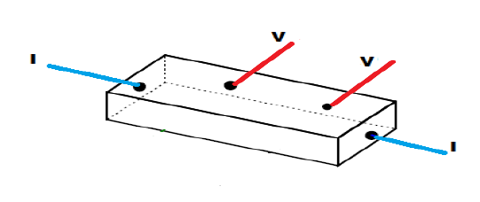
Figure 1. Experimental arrangement of the bar method.
The electrical resistivity of a material is very important for the acceptance of semiconductor compounds, its determination is widely used for quality control purposes. This test method is widely used to make routine measurements. These procedures were initially applied to semiconductors such as silicon and germanium and brought excellent results that contributed to an effective method to measure the resistivity in other semiconductors.
In general, resistivity measurements are more reliable when measured in single crystals, since with this material the variations in impurity that affect the resistivity are lower. Segregation of impurities located in the grain boundaries in the polycrystalline material can lead to large variations in resistivity. Such effects are common to any of the measurements but are more severe with the four-probe method, and their use, therefore, is not recommended for a polycrystalline material
Four-Probe Method
Preparation of the semiconductor sample.
In a publication written by me, explain in detail how a sample of a semiconductor is prepared see here. Although this time I will briefly explain how this sample is prepared to apply the four probe method.
In principle, the sample of the semiconductor compound must be prepared for this method in the following manner:
A small portion of the sample is cut into a parallelepiped.
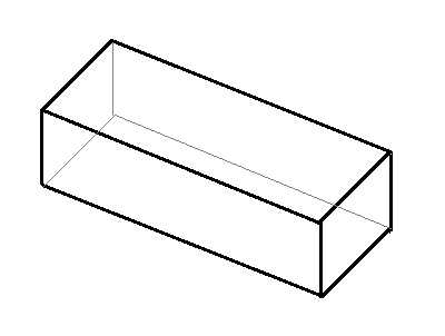
Figure 2. Example of a parallelepiped.
Then it must be polished until it is very bright, this is done so that the measurements do not present significant errors due to the roughness or deformation of the sample, or some other impurity.
Next, the 4 probes or tips must be soldered. In my case I use copper wire, since it conducts the current very well and they are easy to adhere to the semiconductor sample, to make the welding you must use small pieces of indium, which will be heated with a cauting until reaching its melting point where the Indian melts, the fine copper wire is placed at the ends of the sample and an Indian dot is added to hold it.
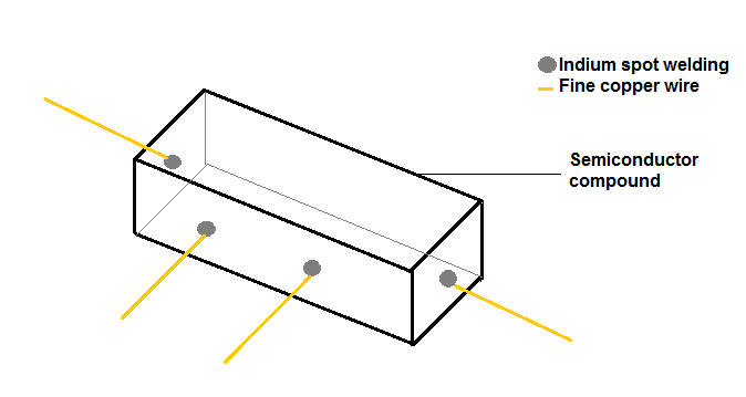
Figure 3. Shows how the indium electrical contacts should be placed in the semiconductor sample.
After having made all the corresponding preparation, the sample should be mounted on a bakelite as shown in the figure. Later the fine copper wires will be connected to a thicker copper wire that is where the current and the voltage of the sample are measured. Bakelite is used as an insulator and as a guide to work comfortably and obtain accurate measurements.
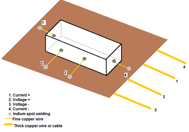
Figure 4. Outline of the sample on bakelite.
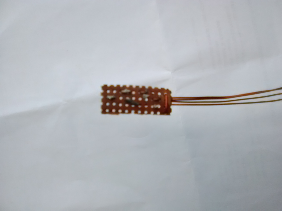
Figure 5. The actual assembly of the sample in Bakelite.
Experimental assembly for the calculation of the electrical resistivity of a semiconductor.
The equipment that is used to perform the measurements of the electrical resistivity of a semiconductor are the following:
Control for temperature
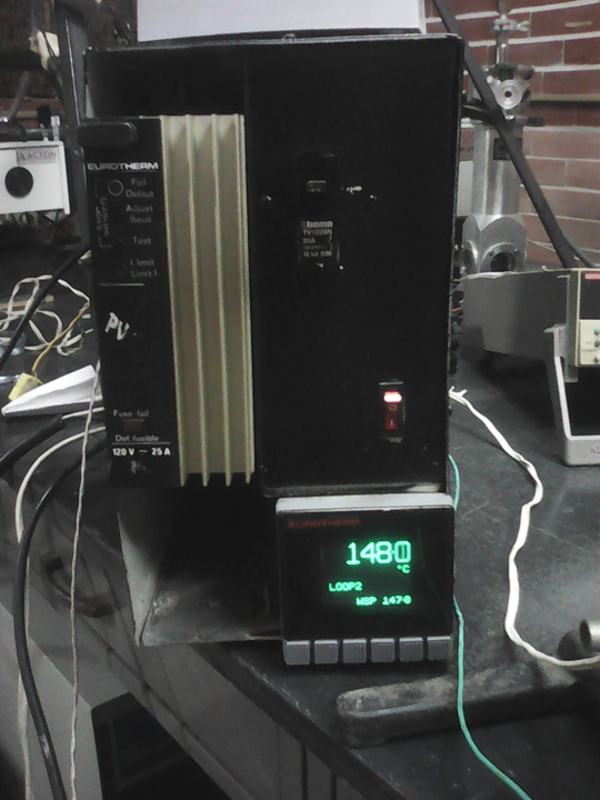
Figure 6. Real photo of temperature control.
As its name indicates, it is used specifically to vary the temperature either increasing or decreasing.
Power supply
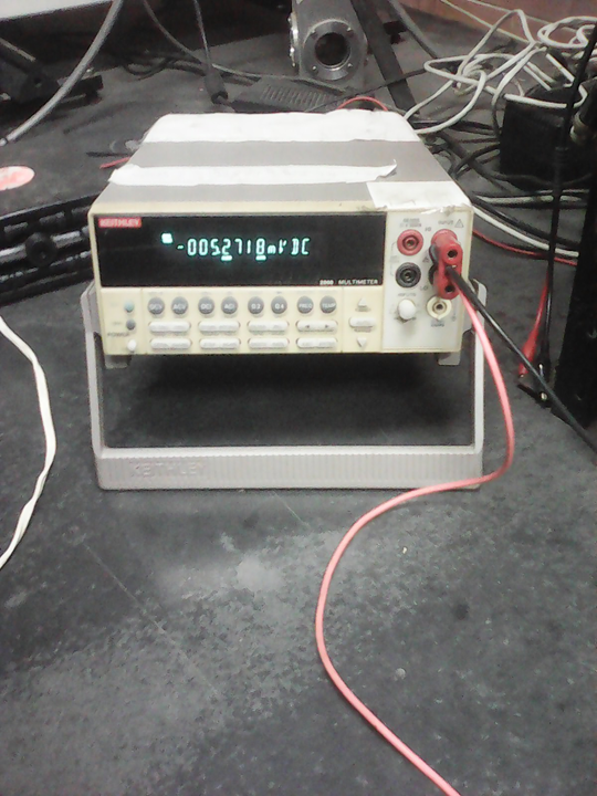
Figure 7. Real photo of power supply.
With this device we collect the variation data of the voltage as a function of the current.
Oven
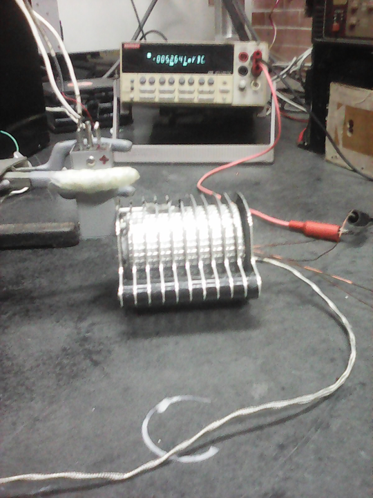
Figure 8. Real photo of over.
In this apparatus, the semiconductor sample to be characterized is introduced, in order to provide the appropriate temperature at the time of measurement.
Current source
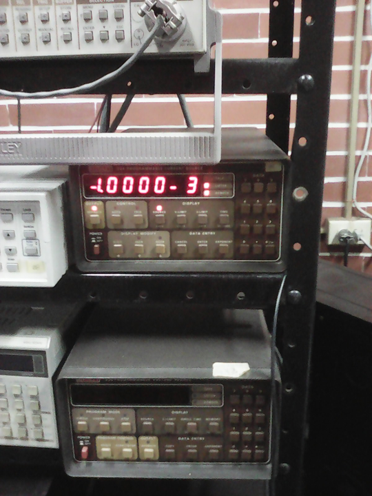
Figure 9. Real photo of current source.
Used to provide current to the sample of the semiconductor compound.
Important
Before carrying out the resistivity experiment as a function of temperature, first of all, it is necessary to verify that the contacts of the sample are ohmic, that is, if there is continuity of current in each of the indium points. For this experimental procedure, a computer program developed in our laboratory is used, configured with Microsoft Exel, where the value of the negative and positive current is recorded, these data will be represented in another computer program and if a Direct line curve is shown that it passes near zero, the law of ohm is fulfilled. This means that the Indian contacts are well elaborated and the next step would be to measure the electrical resistivity as a function of the temperature of the semiconductor compound to be characterized.
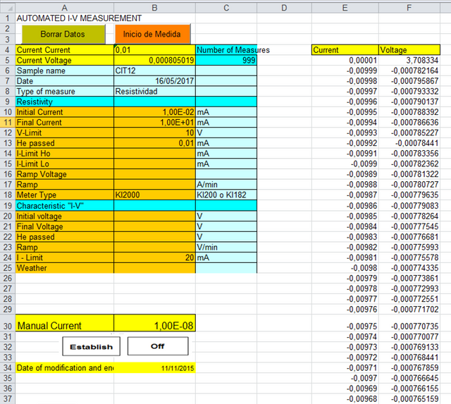
Figure 10. Microsoft Excel software simulation.
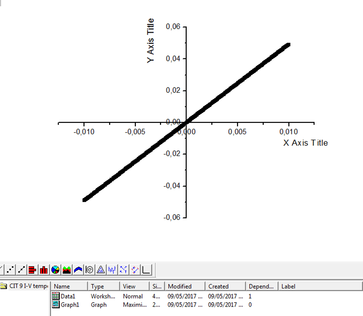
Figure 11. Current vs voltage graph.
The sample is placed in a synthesis oven, current is circulated, then the value of the voltage is recorded at room temperature and the temperature of the sample is increased inside the oven. The value of the voltage and temperature is recorded, the data will be taken. until the Indium contacts are detached from the sample and then the following equation is used to calculate the electrical resistivity:
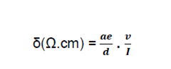
Where: a: is the width of the sample e: thickness of the sample and d: distance of the points.
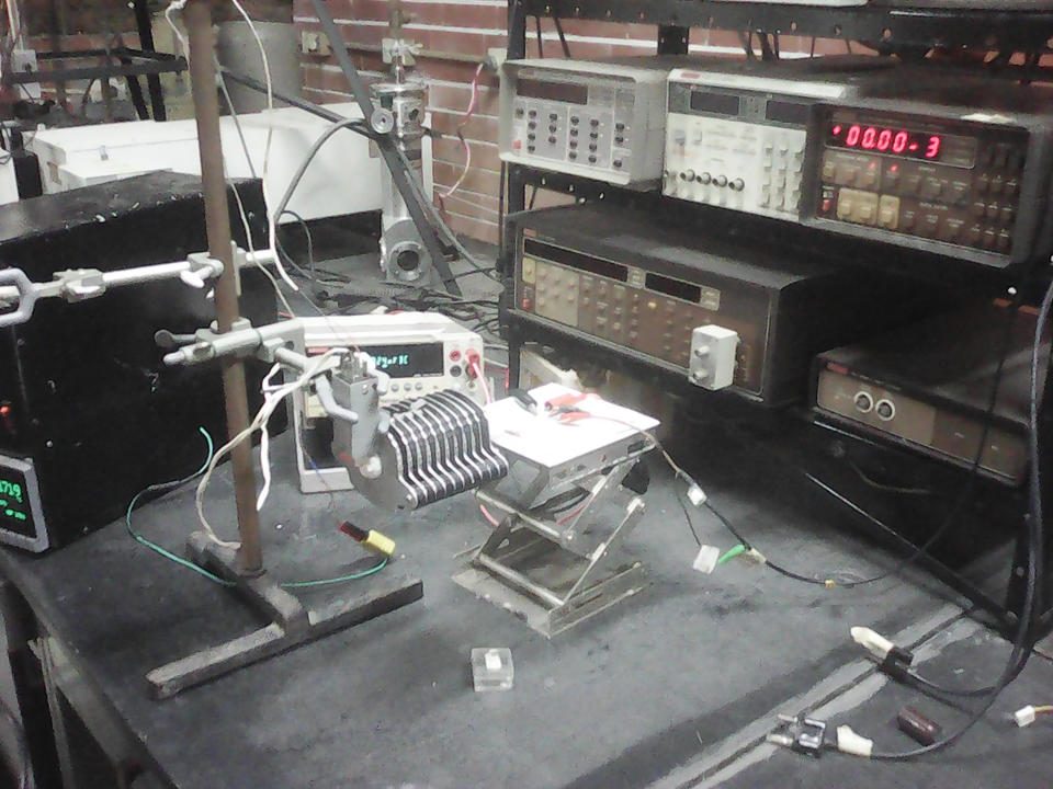
Figure 12. This shows the complete configuration of the experimental assembly for calculating the electrical resistivity as a function of temperature.
Finally, when making the measurements, our computer program configured by Microsoft Exel, will record all the corresponding data of the current and voltage, and finally we can obtain a graph like the one shown in the figure.
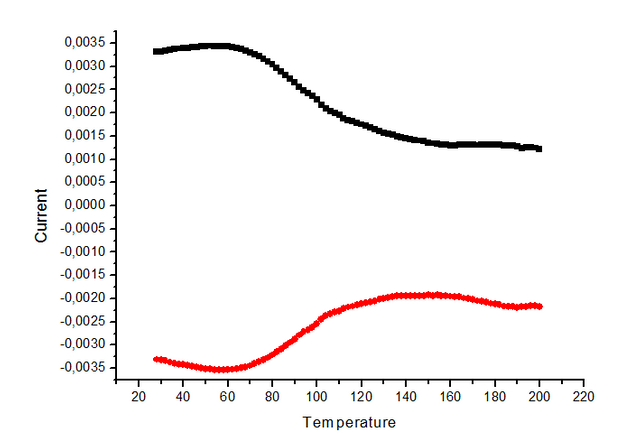
Figure 13. Graph of electrical resistivity as a function of temperature.
References.
Marin, G. (2001). Preparación por diferentes técnicas, estudios comparativos de las propiedades ópticas y eléctricas en función de la temperatura de los semiconductores CuInTe2 y CuGaTe, Tesis de Maestría. Mérida, Universidad de los Andes.
Charles Kittel. Introducción a la física del estado sólido”. Segunda edición. Editorial Reverte.
Smith, W; Hashemi. (2006) Fundamentos de la ciencia e ingeniería de los materiales. Cuarta Edición. México. Editorial McGraw Hill.
ASTMF43-09. International. (2011). Standard (2010) Test Methods for Resistivity of Semiconductor Materials Vol 10.05.
https://es.scribd.com/doc/160020269/Fisica-De-Los-Semiconductores-Shalimova

Wow fantastic stuff. I am going to digest that a while and reread to make sure I got it all! Thanks.
Congratulations @carloserp-2000! You have completed some achievement on Steemit and have been rewarded with new badge(s) :
Click on any badge to view your own Board of Honor on SteemitBoard.
For more information about SteemitBoard, click here
If you no longer want to receive notifications, reply to this comment with the word
STOP