Circuit design using "PSIM" (Buck, Boost and Cuk type regulators to increase efficiency)
I am a student of electronic engineering from the Simón Bolívar University of Venezuela (USB), a few quarters ago I was studying the subject “Electronics of industrial acquisition and processing systems 2” where we were assigned the task of designing a different power supply values using Buck and Cuk type regulators to be used in some blocks of the electric vehicle and increase the efficiency of the converters.
Objectives:
Implementation of feedback loops in the Buck, Boost and Buck / Boost converters to increase their efficiency.
Implementation of an inverter capable of transforming a DC signal to an AC with a variable frequency.
Specifications:
Acquisition Stage:
• 24 V @ 200 mA.
• -24 V @ 200 mA.
• 5 V @ 100 mA (95% efficiency).
Processing Stage:
• 3.3 V @ 10 mA (95% efficiency).
 • 5 V @ 1 A.
Actuators stage
• Traction 48 V peak-peak @ 5 A. with a variable frequency of 40 Hz to 60 Hz.
• Mirror movement: 5V @ 500 mA.
Procedure and Results:
The idea of feedback is to improve the efficiency of the power supply since, if variations of the input signal occur, the system reacts to compensate for such variation, if the signal decreases, the controller would increase the duty cycle to keep the power constant exit sign.
A PWM control system per voltage and current sample will be used as appropriate.
The PWM control per voltage sample where the sample signal is compared with a reference voltage, the value of which depends on the magnitude desired at the output. The comparison uses a triangular signal whose duty cycle will depend on what is requested at the output and whose frequency is also set.
The PWM control per current sample where the sampling signal is the current. The current signal will be taken from the inductor since there are the maximum variations of the current. For this control, the same applies to the PWM control per voltage sample with the difference of taking a reference current instead of a voltage.
For the DC-AC conversion where the configuration will be single phase, where there are two switches (MOSFET) that will act as a “switch” implementing two states (one on and one off or vice versa). The waveform generated by a single phase inverter is a square of maximum values Vcc / 2 and –Vcc / 2 respectively.
Acquisition Stage:
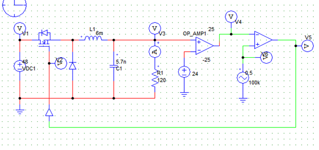
Regulator to get 24V @ 200mA:
The use of the differential amplifier is to fulfill the following relationship:
V4 = G * (Vo-Vref), where G is the amplification of the error obtained at the output. The triangular source value will have the switching frequency (100Khz) and the duty cycle value k (0.5).
For the switching frequency at 100Khz, a maximum value of 20 mA and 2.4V of curling, an inductor value of at least 6 mH and greater than 10.42 nF is required.
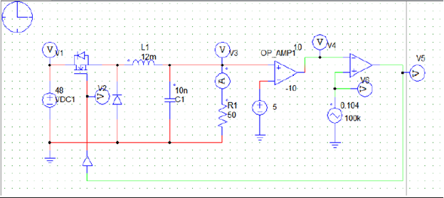
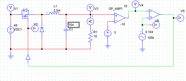
5V @ 100mA regulator.
The use of the differential amplifier is to fulfill the following relationship:
V4 = G * (Vo-Vref), where G is the amplification of the error obtained at the output. The value of the triangular source will have the switching frequency (100Khz) and the duty cycle value k (0.104).
For the switching frequency at 100Khz, a maximum value of 10 mA and 5mV of curling, an inductor value of at least 12mH and greater than 250nF is required.
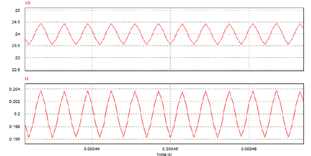
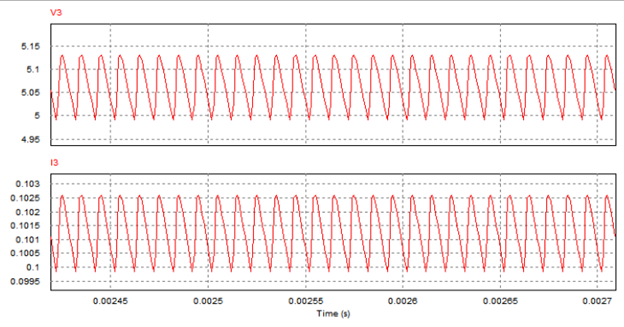
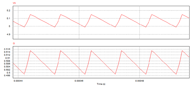
They are shown below:
They are shown below: Upper graph (V3): Output voltage.
Lower Graph (I3): Output Current:
Processing Stage:
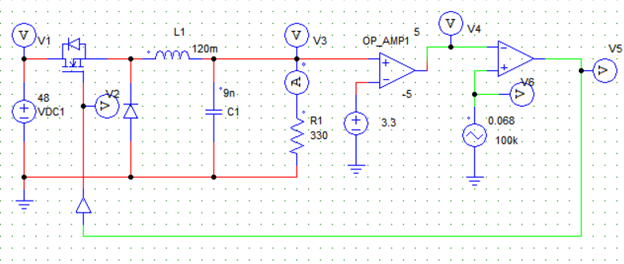
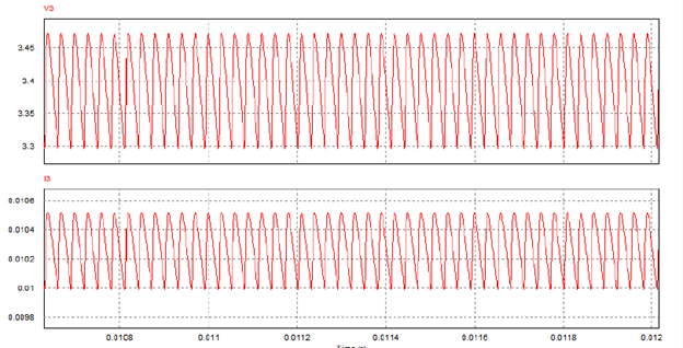
Regulator to get 3.3V @ 10mA.
The use of the differential amplifier is to fulfill the following relationship:
V4 = G * (Vo-Vref), where G is the amplification of the error obtained at the output. The value of the triangular source will have the switching frequency (100Khz) and the duty cycle value k (0.068).
For the switching frequency at 100Khz, a maximum value of 1 mA and 33mV of curling, an inductor value of less than 120mH and greater than 37nF is required.
Upper Graph (V3): Output Voltage:
Bottom Graph (I3): Output Current:
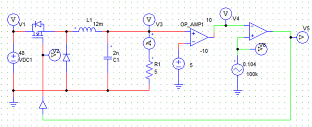
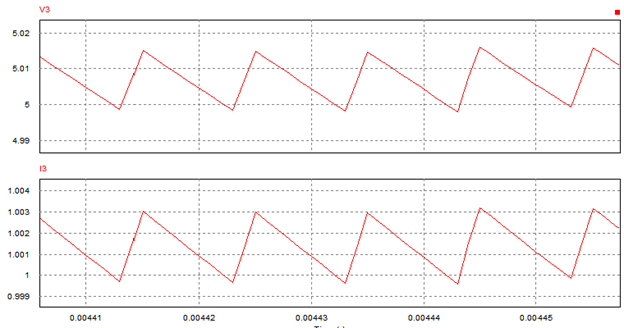
Regulator to get 5V @ 1 A:
The use of the differential amplifier is to fulfill the following relationship:
V4 = G * (Vo-Vref), where G is the amplification of the error obtained at the output. The value of the triangular source will have the switching frequency (100Khz) and the duty cycle value k (0.104).
For the switching frequency at 100 Khz, with a maximum value of 10mA and 250 mV of curling, an inductor value of less than 12mH and greater than 50nF is required.
Upper graph (V3): Output voltage.
Lower Graph (I3): Output Current.
Traction stage:
Regulator to get 5V @ 500mA:
The use of the differential amplifier is to fulfill the following relationship:
V4 = G * (Vo-Vref), where G is the amplification of the error obtained at the output. The value of the triangular source will have the switching frequency (100Khz) and the duty cycle value k (0.104).
For the switching frequency at 100Khz, a maximum value of 50 mA and 250 mV of curling, an inductor value of at least 2.4 mH and greater than 250nF is required.
Upper graph (V3): Output voltage.
Texto
Lower Graph (I3): Output Current.
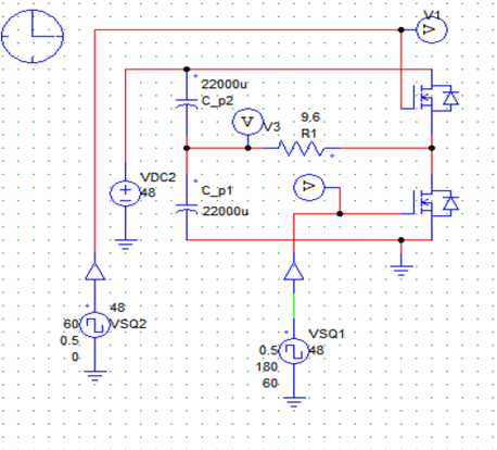
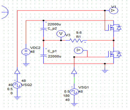
Traction 48Vp-p @ 5 A with frequency between 40 Hz and 60Hz:
For the single-phase inverter a symmetric signal of 24 Vp or 48 Vp-p is desired. Square signal controllers that operate with a 50% duty cycle will be applied in order to make the output signal symmetrical. The phase of a generator will be 0 ° and the other 180 ° with a maximum output voltage. ¨ Finally, the values of both capacitors will comply with the relationship Vc (t) = Vcc / 2. Since 24 F is very large, we will take 22000uF.
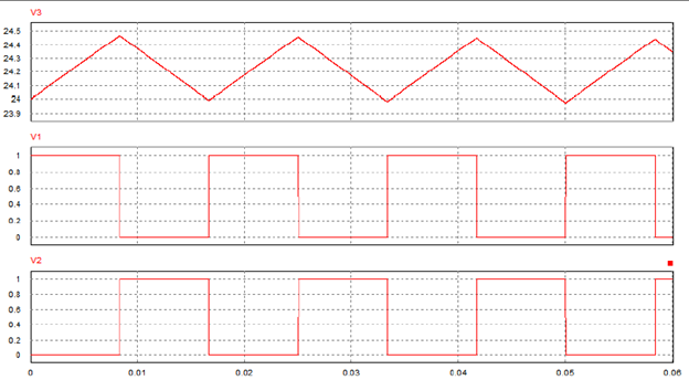
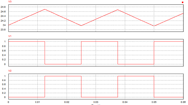
At 60 Hz:
Upper graph (V3): Output voltage.
Intermediate Graph (V1): Square signal with alpha = 0 °.
Lower Graph (V2): Square signal with alpha 0 180 °.
At 40 Hz:
Upper graph (V3): Output voltage.
Intermediate Graph (V1): Square signal with alpha = 0 °.
Lower Graph (V2): Square signal with alpha 0 180 °.
This post was shared in the Curation Collective Discord community for curators, and upvoted and resteemed by the @c-squared community account after manual review.
@c-squared runs a community witness. Please consider using one of your witness votes on us here
Hello @orbital753, thank you for sharing this creative work! We just stopped by to say that you've been upvoted by the @creativecrypto magazine. The Creative Crypto is all about art on the blockchain and learning from creatives like you. Looking forward to crossing paths again soon. Steem on!