SEMICONDUCTORS: THE BASICS OF ALL ELECTRONICS AND INVENTIONS #4
The world of engineering and technology keep advancing every day, but people tend not to know and understand the start, the basics and the genesis of this great adventure.
I keep on wandering, how do we come about all these electronics and gadgets, I asked myself so many questions, is this part of the miracles and wonders of the old experienced by fore-fathers, are electronics made through magic and incantations, no, it should be by invoking spirits of dark powers. Source: Episode 1
Don't forget to visit episode 1, episode 2 and episode 3 of this write-up.
Fabrication of semiconductor devices
Semiconductors devices such as Integrated circuit (IC), transistors, diodes, resistors, and capacitors are fabricated through series of processes.
Today I will take us through how to fabricate an Integrated circuit, and enlighten us on the technology behind engineering an IC .
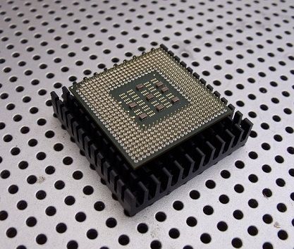
Integrated circuit is a miniature device which is actually packed with billions of electronic components such as transistors, diodes, resistors, and capacitors, they all work together to perform logical operations and also store sets of commands or instructions to be executed.
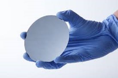
In an integrated circuit or monolithic IC also known as microchip, all the circuit components involved in fabricated are manufacture into or top of a block of silicon which is known to as chip or die. It is a semiconductor wafer in which millions of components are fabricated. Metallization patterns are required to make interconnections between the components present inside the chip as a single thin wafer (substrate) called monolithic IC. The individual components of a microchip are not separable from the IC circuit.

What is Silicon?
By mass, Silicon is the eighth most common element in the universe, it is about 27.7% part of the earth crust. Silicon is the second most abundant element after oxygen, it is generally distributed in dusts, sands, planetoids and planets as various forms of silicon dioxide (silica) or silicates. It’s rarely occurs as pure free element in nature.
Silicon is the primary component of most semiconductor devices, most importantly Integrated circuit or microchips. On the basis of its characteristics, silicon is widely used in semiconductor production industries. At present, silicon-made devices constitute over 95% of all semiconductor devices.
The various processes and steps involved in fabrication of silicon devices or semiconductor devices are listed below:
- Silicon Substrate Preparation
- Chemical Vapour Deposition (CVD)
- Oxidation
- Photolithography
- Diffusion
- Ion Implantation
- Metallization
At the moment, I will take us through how to prepare silicon substrate.
There we go.
Silicon substrate preparation has been structured into four sections as follows for effective reading:
- How to prepare electronic grade silicon
- Czochralski Crystal Growth Process
- Wafer preparation
- Wafer processing
How to prepare electronic grade silicon
Semiconductor devices demand a very pure form of silicon known as electronic grade silicon which can be achieved through series of processes. Electronic-Grade Silicon (EGS) is a high purified polycrystalline substance which serves as the raw material used for the preparation of single-crystal silicon. EGS contains some major impurities like carbon, boron, and residual donors.
The doping elements of pure EGS are expressed in parts per billion (ppb) range, and carbon less than 2 parts per million (ppm).
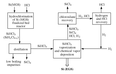
The step by step procedure involved in EGS preparation are described by the block diagram below.
Synthesis and purification of bulk polycrystalline semiconductor material to produce electronic grade silicon EGS represents the first step towards the commercial fabrication of an electronic device in which quartzite gravel is a typical source material for commercial production of elemental silicon.
synthesis and purification of polycrystalline semiconductor material
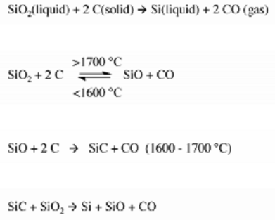
Metallurgical Grade Silicon (MGS) is produced by charging quartzite gravel with carbon in a submerged-electrode arc furnace along with the appropriate chemical reactions, carbon serving as an electrode. In the arc furnace, the reaction convert silica to silicon at temperatures over 1,900 °C(3,450 °F). Carbon can be obtained in the form of coal, coke, and wood chips while a Quartzite is obtained from sand which is a relatively pure form of sand (SiO2).
The overall reaction for the process is shown below:
The result of this reaction produces a Metallurgical-grade silicon (MGS) that is 98% pure, this purity is not suitable enough to fabricate a semiconductor device, because small amounts of some impurities such as aluminum and iron which are the major impurities have a strong influence on the electric characteristics of a semiconductors, it is required that the bulk raw material must be of very high purity (> 99.9999%). Therefore MGS is needed to be pulverized mechanically after which trichlorosilane (SiHCI3) is formed by reacting it with anhydrous hydrogen chloride (HCI).
Chlorosilane (Seimens) process
The basic concept of which involves the conversion of MGS to a volatile silicon compound.
Trichlorosilane is synthesized by heating powdered MGS with anhydrous hydrogen chloride (HCl) at a temperature around 300 ◦C in a fluidized-bed reactor.
The reaction is shown below.

Since the formation of SiHCl3 highly exothermic, efficient removal of generated heat is essential to assure a maximum yield of SiHCl3.
Purification of trichlorosilane
The purification process is done by fractional distillation method because the trichlorosilane and impurities of chlorides which are liquids at room temperature such as iron, aluminum, and boron are removed as FeCl3, AlCl3, and BCl3, respectively. Fractional distillation of SiHCl3 from these impurity halides result in greatly increased purity with a concentration of electrically active impurities of less than 1 ppb.
The purified SiHCI3 is then subjected to chemical vapor deposition (CVD) such as Silicon epitaxial layer on a single-crystal silicon substrate (homoepitaxy or commonly referred to as epitaxy). Silicon tetrachloride and its lower chlorinated derivatives are used for the chemical vapor deposition (CVD) growth of Si and SiO2.
The high-purity SiHCl3 is vaporized, diluted with high-purity hydrogen, and introduced into the Seimens deposition reactor.
The chemical reaction involves a hydrogen reduction of SiHCl3 as shown below.
2SiHCl3 + 2H2 = 2Si + 6HC
This reaction results in production of EGC rods which are raw materials for the formation of single crystal material that is processed to semiconductor wafers.

Schematic representation of the reaction pathways for the formation of EGS using the chlorosilane process.
Adapted from
The alternative method of producing EGS is pyrolysis method, It involves reaction of silane(SiH4) with heat which takes place at a high temperature of 900 ◦C.
Using saline instead of trichlorosilane lowers production cost associated with lower reaction temperatures and also reduces the production of harmful reaction and by-products.
SiH4 + HEAT = Si + 2H2

It was noticed that SiHCl3 is predominantly used in synthesis of EGS even though pyrolysis method reduces cost of production associated with lower reaction temperatures. Reasons for this are highlighted below:
Reasons for the predominant use of SiHCl3 in the synthesis of EGS
The reasons for the predominant use of SiHCl3 in the synthesis of EGS are as follows:
- SiHCl3 can be easily formed by the reaction of anhydrous hydrogen chloride with MGS at reasonably low temperatures (200 - 400 ◦C).
- It is liquid at room temperature so that purification can be accomplished using standard distillation techniques.
- It is easily handled and if dry can be stored in carbon steel tanks.
- Its liquid is easily vaporized and, when mixed with hydrogen it can be transported in steel lines without corrosion.
- It can be reduced at atmospheric pressure in the presence of hydrogen.
- Its deposition can take place on heated silicon, thus eliminating contact with any foreign surfaces that may contaminate the resulting silicon and
- It reacts at lower temperatures (1000 - 1200 ◦C) and at faster rates than does SiCl4.
Series of this write-up will be many because I decided to compile all these posts as a lecture note for my students, so, for easy understanding of all procedure and processes involved, I will not want to miss out any important aspect of this write-up.
Hope you are getting along with knowing the technology behind engineering an IC.
Thanks for your time
Don't miss the next episode

Interesting post
this is truly nice Mr. Ola.
from @steve1122 (C.M)
thanks @steve1122
pleasure is all mine, nice to meet you @rubies have heard a lot about you..
World of discovery.Am getting fascinated to the world of physics through your post.
Thanks my brother, Physics is an expression of our day to day life