SEMICONDUCTORS: THE BASICS OF ALL ELECTRONICS AND INVENTIONS #3
The world of engineering and technology keep advancing every day, but people tend not to know and understand the start, the basics and the genesis of this great adventure.
I keep on wandering, how do we come about all these electronics and gadgets, I asked myself so many questions, is this part of the miracles and wonders of the old experienced by fore-fathers, are electronics made through magic and incantations, no, it should be by invoking spirits of dark powers. Source: Episode 1
The last episode explained that semiconductors are neither insulators nor conductors but a material whose resistivity (10E-4 to 0.5 Ωm) lies in between insulators and conductors, then why don't we classified a semiconductor as a resistance material? That is the question. Answer shall be made available shortly, just stay with me.
Source: Episode 2
I advise that you read through previous episodes to have a clear understanding of the subject to be considered in this episode. Visit to read Episode 1 & Episode 2
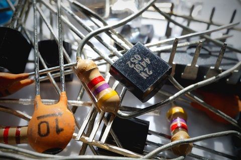
A integrated circuit (IC), also referred to as a semiconductor chip is an electronic device packed with billions of electronic components such as resistors, diodes, transistors, and capacitors. All these components work together to perform logic operations which logically execute stored commands and instructions.
Today, I am introducing a new series of my post that will walk you through the entire fabrication process of semiconductor devices, from the raw material stage to the final testing of the semiconductor chip.
Most semiconductor devices such as integrated circuit (IC), transistors, diodes contain one or more p-n junctions, therefore, before going into the details of the technology behind engineering an IC, we have to consider the fabrication of p-n junction.
p-n junction Fabrication made easy.
Do you know that you can actually manufacture p-n junction yourself? Simply sit back, read and understand the following explanations.
When a p-type semiconductor is suitably joined with a n-type semiconductor, the point of contact of the two surfaces is referred to as p-n junction. Most semiconductor devices contain one or more p-n junctions, whose effects is of most important because it serves as the control element for semiconductor devices. In actual practical sense involved in the formation of p-n junction, its characteristic properties will be a flaw if a p-type block is just made in contact with n-type block.
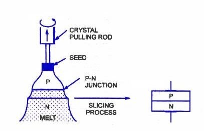
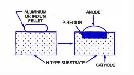
Fabrication of p-n junction is achieved through special techniques but the common method or technique is called alloying. Using method of alloying, small block of indium which is a trivalent impurity will be placed on an n-type germanium slab. The system is then heated to a temperature of about 500 degree centigrade. At this temperature, the indium and some part of the germanium slab melt to form molten germanium-indium mixture. At lower temperature, the mixture begins to solidify. Under a suitable condition, the atoms of indium impurity will be suitably adjusted in the germanium slab to form a single crystal. The reason for adding indium impurity is to overcome the excess electrons in the n-type germanium such that it create a p-type region.
Immediately the p-n junction is formed, the free electrons close to the p-n junction in the n-region diffuses through the junction into the p-region where they interact and combine with holes close to the junction. This result that n-region loses free electrons as diffusion occurs at the junction. This creates a layer of positive charges which are pentavalent ions near the junction. The p-region loses holes as the electrons and hole combine, when electrons move across the junction. This result in the creation of a layer of negative charges which is a trivalent ions near the junction.
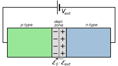
A layer formed by the combination of the two layers of positive and negative charges is called depletion region or depletion layer and an electronic device formed by this technique is referred to as alloy-type or fuse junction diode. The term depletion is used because the layer formed is empty of charge carriers that is, no available free electrons and holes due to diffusion across the junction. The depletion region is very thin compared to the n-region and p-region.
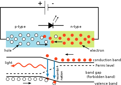
Congratulations, you just fabricate your first semiconductor device called fused junction diode. A Diode is a p-n junction electronic device that allows currents to flow in one direction only, it consisting of a p-region and n-region. The p-region is the positive terminal and n-region is the negative terminal of the diode. With suitable biasing method, you are good to use your diode.
This brings us to the end of the first series of this work. Want to know what happens next? Then, stay tuned for the next series of this post, as I will take you through the details of the technology behind engineering an Integrated circuit (IC).
Thanks for your time
Thanks for sharing. Educative
Thanks, expect more of educative posts in this series
Hello to all. If you're tired of using low-quality vacuum cleaners that leave your floors half-clean and cause more frustration than cleanliness, you should consider the devices that the Hoover brand offers. With over a century of history, the company is a pioneer in the cleaning industry, continually offering exceptional products that revolutionize the way we do household chores, and if you call hoover customer service they will help you find the unit that's right for you.