Project // Digital Odyssey - Part 3: Bit Arithmetic and Venn Diagrams

Project // Digital Odyssey
From 'Bits' to 'Hello World'... and Beyond.
Chapter I - Hardware and Theory
Part 3: Bit Arithmetic and Venn Diagrams
As promised in the last part, in this section I will present to you how to build your own bit arithmetic components from basic logic gates. Check out the Table of contents for a project introduction.
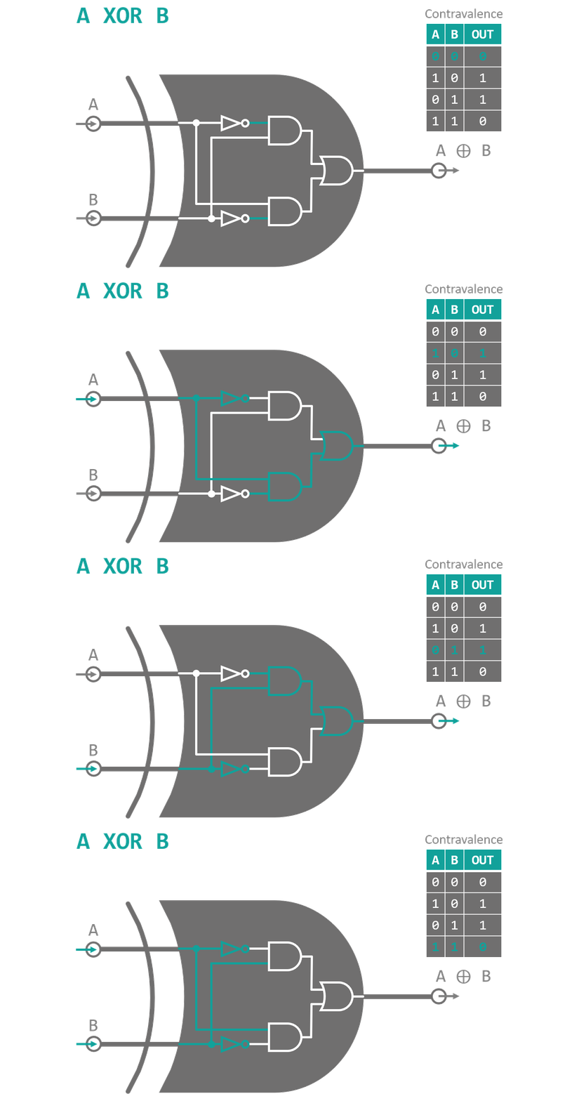
Before we start building our first bit arithmetic circuit, we need to take a look at two more logic gates. The first one is another member of the 'two input, one output' group of gates. It is called XOR (short for exclusive or) gate and represents the contravalent Boolean operation. Contra is the Latin word for against and valent is the third person singular of valere which means being worth and is also root of the word value. It therefore translates to something around the lines of with non-similar values. Hence, a XOR gate only outputs a high value if both of its inputs have opposite values. To figure out how to build a XOR gate from AND, OR and NOT gates, which we have discussed in Part 2, we take a look at the gate's output values. The two input configurations that lead to a high output state are 'A=1, B=0' and 'A=0, B=1'. These statements can be expressed as 'A AND (NOT B)' as well as '(NOT A) and B'. Finally, we combine the two subexpressions using the OR operation to find:
This way of decomposing logic relations into ANDs, ORs and NOTs is called the disjunctive normal form (DNF) and it is quite handy for constructing unknown logic operation where you are only given the configuration tables. Wolfram Alpha provides a nifty web calculator that displays truth tables, all kinds of decomposition and visualizations [1]. Figure 1 shows a circuit diagram using the DNF to build a XOR gate.
For completeness sake: Contravalence is the inversion of equivalence where equi means same or equal (which should be quite obvious since they share the same root word). We call the inverted XOR gate a XNOR (exclusive not or) gate and it outputs a high value when both inputs are equal to each other.
It is time for our obligatory detour: If you are still struggling to grasp the concepts of Boolean logic or just want to see a different approach, a nice way of visualizing the effect of Boolean operations are Venn diagrams. Boolean algebra not only applies to binary logic as in 'pushing bits around' but also to set theory i.e. the science of what elements belong to which sets. A set is a collection of any number of distinct objects. You can group numbers, colors, animal names or your favorite generations of charged Dirac-Fermions... you name it, sets contain it. Boolean operations on sets ask questions about whether elements belong to a set or not (here the binary or two valued aspect of the matter comes into play). Let's apply, what we already know about Boolean operations. Take for example the negation operation (NOT gate). The inverse of a set A contains all elements that are not part of A. Example: Our distinct objects shall be the numbers 1 to 10. A set - let's call it O - might contain all odd numbers {1,3,5,7,9}. The inverse of O - denoted O̅ - is the collection of everything else that is not element of O i.e. {2,4,6,8,10}. The Venn diagram of this relation as well as all other single input Boolean operations can be found in figure 2. The diagrams contain two parts: A circle, representing the input set, which we apply our operation on and a surrounding box which makes up everything else that is not element of this set. The parts of the Venn diagram that are highlighted are the ones contained in the output set of the Boolean operation.

Next step: Two input Boolean operations like conjunction (AND gate) or adjunction (OR gate). A complete list of all two-input Boolean operations and their Venn diagrams is given in figure 3. Again, the input sets are represented by circles and the rest of the elements is contained in a surrounding box. However, there is a forth part added to the diagram: No one restricts us to putting our elements into one set exclusively. An object can be element of multiple sets at the same time. The number 6 for example is element of the set of all even numbers but it is also element of the set of all numbers that are integer multiples of 3. In this sense, our two-input Venn diagram contains an overlap area between the input sets, representing all objects that are element of both inputs. Using this visualization, the terms conjunction from Latin conjugere 'to merge' and disjunction as in 'to separate' become more obvious as they are used in their literal meaning. The inverse operations NAND (everything that is not element of the overlap of A and B), NOR (everything that is neither A nor B - the word even found its way into the English language) and XNOR (everything that is either element of both A and B or element of none of them) should become more clear as well from looking at the diagrams.
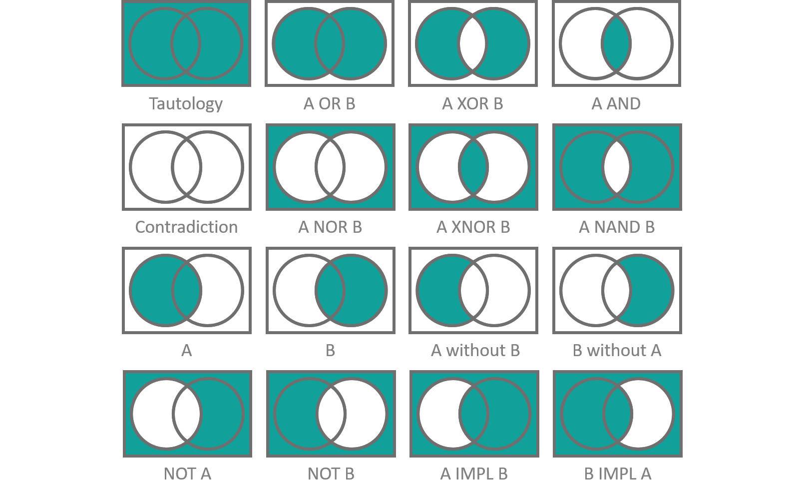
The only Venn diagrams that struck me as not being immediately comprehensible are the implications 'A IMPL B' as well as 'B IMPL A'. 'A implies B' translates to, "when the object is not element of A then it can be element of anything else, or when it is part of A it must be part of B as well". In terms of sentential logic an implication is a funny construct. Especially, when A is not true, B can be either true or false and the statement will still be true in the end. For example: "The fact that Ben visits us tomorrow and does not visit us tomorrow implies that all cows are green". This statement (although it does not make any sense) is TRUE, even though, clearly not all cows are green. The first part "Ben visits us tomorrow and does not visit us tomorrow" is a contradiction since both events negate each other and therefore it yields a false result either way. Since the first part of the statement cannot become reality the result of the second part "all cows are green" does not change the truth content of the implication. It is true no matter whether all cows are green or not, since a false implication does not allow us to make any prediction about the outcome of what we try to imply. Admittedly, this example is pretty stupid, but it shows a very crucial aspect of logic: A false statement implies something that is true, even if the implication is false as well. The peril lurks in implication where we cannot simply identify the first part as being false as easily. Utter nonsense can be proven true using implications from statements that are designed to look credible but contain hidden contradictions. Most conspiracy theories work that way. They might be intrinsically consistent, convincingly following all rules of logic to prove the wildest theories, however they are based on one or more false initial assumption that cannot be debunked on a first look. A company might promise their product does literally wonders to your carpet, but there will be a small asterisk pointing to a footnote stating, that this is only accomplished when Snow White and the seven dwarfs are invited to a tea party in Alice's wonderland where everyone decides to help with the cleaning of your floor using the advertised product. The moral of this story? Always have a very close look at the initial assumption before believing an implication. Also be careful, implications are not reversible! If A implies B, this does not automatically mean that B implies A. Just because it is true that "if it rains, the lawn gets wet", there is no need to demand that a wet lawn implies a rainy day... maybe it's just your caretaker using a sprinkler on a hot sunny summer day.

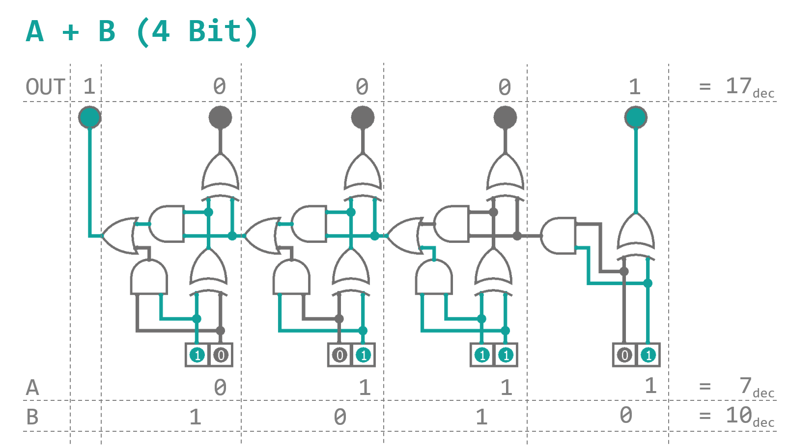
Ok, back to binary arithmetic. We are now given all necessary components to build the core of our first binary arithmetic operation: The Addition. Let us quickly remember, how we added two numbers before we were allowed to use a calculator. Both numbers were written down, aligned at their lowest (rightmost) digit. Then, starting from the right, the sum of two digits on top of each other was taken and the resulting digit was appended to a third row. Any overflow was added to the summation of the next digit pair to the left. See figure 4 for an example. Good news: This method is applicable to binary numbers absolutely identically. When summing over the rightmost column the possible results are:
Observe the behavior of the first digit of the results. It is only 1, when either of the inputs is 1 and 0 otherwise. This should ring a bell... exactly, that's where we are going to use our first XOR gate. The overflow into the next column is 1, when both inputs are 1 simultaneously... seems reasonable to use an AND gate here. The next column is a little more complex as it requires the summation over three input bits, taking the overflow into account. This can be achieved by stacking two 2‑bit adders - similar to the one used for the first row - behind each other. Every subsequent row afterwards is just a repetition of this component. The whole setup is known as a binary full adder and can be seen in figure 5. It was created and simulated using a software called 'Logisim', which is freeware and can be found here [2]. I strongly encourage you to go ahead and play around a little, if you are unfamiliar with the whole logic business.
The next operation we are going to build is: The Subtraction... done! 'Wait, what?' We do not need to build a dedicated subtraction component as both operation can be performed using the full adder. All we need is a clever way of expressing 'negative' binary numbers using a fixed number of bits. The most straight forward approach would probably be to use the leftmost bit as a sign bit differentiating positive and negative numbers (like 0011 = 3dec and 1011 = -3dec). This, however, makes implementing the addition and subtraction using the same component nearly impossible. Also, it yields a positive and a negative representation for the number 'zero' (0000 = 1000 = ±0dec) which does not make much sense. A better solution is the so-called two's complement: Take any binary positive number with a fixed number of bits, say 0011 ( = 3dec), negate all digits (1100 = 12dec) and add 0001 to the result (1101 = 13dec). How does this help? When the positive number and its two's complement are added (0011 + 1101) the result by design yields the next power of two (10000 = 16dec = 24), since we are looking at binary numbers with fixed length, the final overflowing bit cannot be taken into account and the result is truncated to 0000. Even though, 1101 is a positive 4‑bit number it is also the solution of the equation 0011 + X = 0000. Hereby follows that 1101 can be interpreted as -0011. This works out because adding a number to its inverse version yields something with all n digits set to 1 (either of the input digits will be 1, the other 0 and 1 + 0 = 1 as well as 0 + 1 = 1). Adding another 1 to the right makes all bits flip as the overflow from adding 1 + 1 = 10 travels through the digits like falling dominos, leaving everything zero but the final overflow. On a more algebraic level, the inversion of a n‑bit binary number turns out to be equivalent to
Resolving this for 2n gives the recipe for finding the two's complement as written above (‑A ≡ A̅ + 1). See figure 6 and check it for yourself if you like. This way of representing negative binary numbers also solves our issues with 'zero' as the two's complement of 0000 conveniently stays 0000.

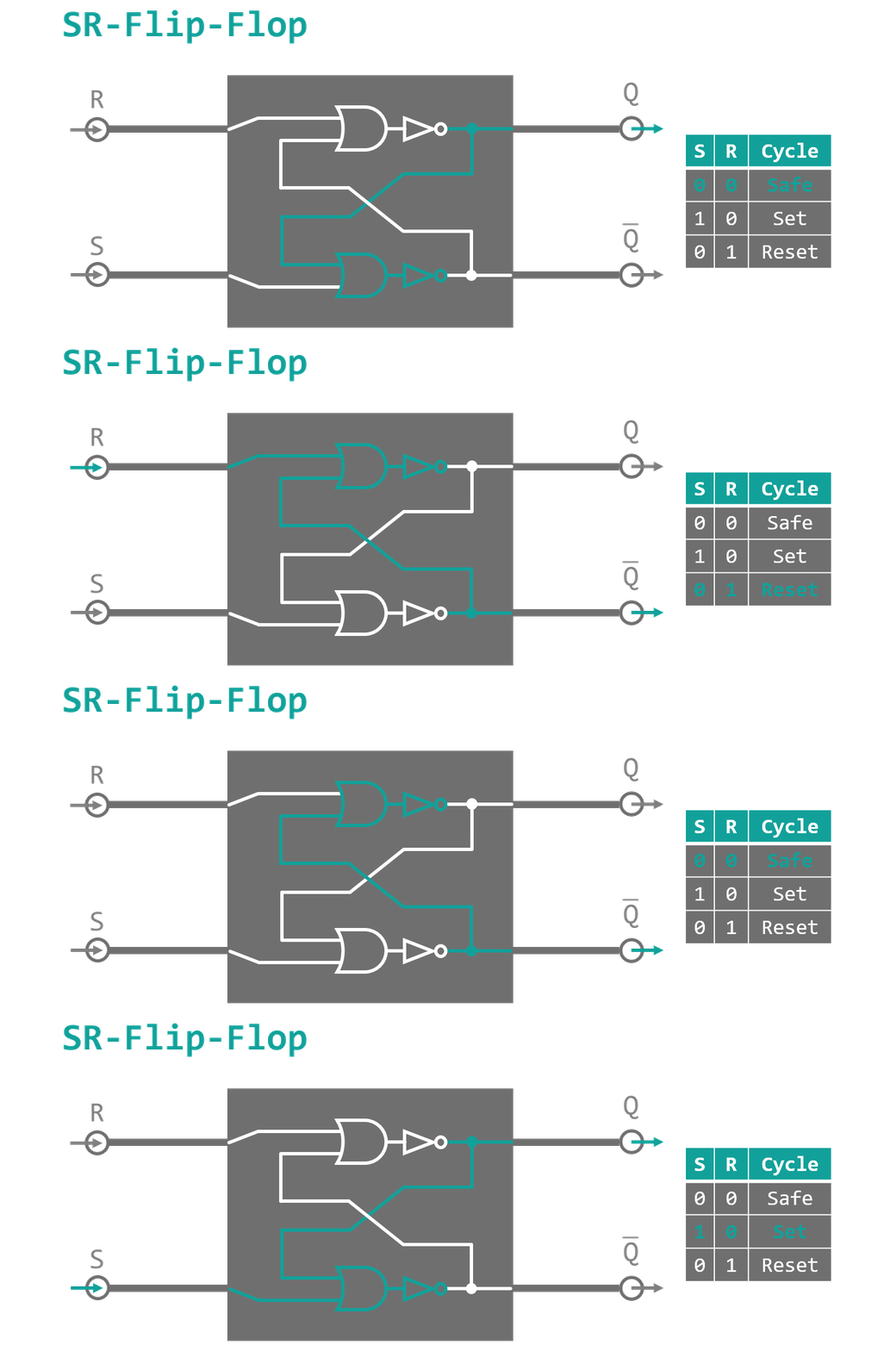
Those of you who have not fallen asleep, yet, might have noticed, that a) I dubbed the full adder presented in figure 5 ominously 'the core' of the instruction and b) I claimed that for the full blown thing we needed two new logic gates, of which I have only introduced one (the XOR gate) so far. So finally here it is, the long awaited second gate: The SR-Flip-Flop. 'Summery beach footwear as electronic components? Has he finally lost it?'. No, not this kind of Flip-Flop of course. Flip-Flop or latch is the name of a bistable (that means stable in two distinct configurations) logic component, a basic one‑bit memory cell if you so will. A very simple variant is the SR-Flip-Flop as depicted in figure 7. It consists of two NOR (not OR) gates with crossed feedback lines and two in- and two outputs. The inputs are called S (for SET) and R (for RESET) and toggle the internal state of the Flip-Flop towards its 'high' or 'low' configuration on a high signal. In the 'high' state the output Q is high and the second reversed output Q̅ yields a low signal and vice versa in the 'low' state of the cell. When none of the inputs is high, the feedback ensures, that the internal state stays as it is (until someone turns off the device and the power cuts out). When both inputs are high at the same time, the Flip-Flop does not know what to do and starts crying... so don't do that.
By adding an AND gate in front of each of the SR-Flip-Flop's inputs, we end up with something called a gated SR-Flip-Flop. One of the inputs of each AND gates will act like the SET and RESET line of the original Flip-Flop. The remaining two inputs are joined into a single connection. SET and RESET can only propagate to the memory cell, when this third input is set high at the same time, like a triggering mechanism. Finally, instead of having two inputs (SET and RESET) separately, we derive both signals from one common data input. SET will follow the data signal via a buffer gate which simply repeats its input value. The RESET line on the other hand will be fed through a NOT gate. This way, when the data input is high, SET is high and RESET is low and the other way around for a low data input. The buffer gate is added as a precaution to match the short delay of the NOT gate, to ensure both signals will arrive with the same trip time. When the trigger fires, both AND gates open and the SR-Flip-Flop sees either of it's inputs in a high state, toggling its internal state according to the data feed. The whole setup is called a gated d-latch (d for data). It has a data and a trigger input and will be used in an input cache for our binary adder.
Why exactly do we need an input cache when the full adder adds numbers just fine without it? All instructions of our processor will be divided into three phases described in table 1. We need to store at least the input as the operands and the results will not be accessed at the same time.
| # | Name | Description |
|---|---|---|
| Through a main data input, the operands for the instruction are loaded into an input cache. | ||
| Give every bit a little time to get comfortable and settle into the instruction until a result precipitates out. | ||
| The output of the instruction is withhold by AND gates which receive a high signal in this phase and release the result of our operation into the main data output line of the processor. |
Putting all pieces of our 4‑Bit ADD instruction together, we end up with a binary device with 2 × 4 input bits (the two operands) 2 trigger inputs (one for writing the input cache, one for reading the output) and 4 output bits (carrying the sum of the two operands). The whole contraption can be seen in figure 8.
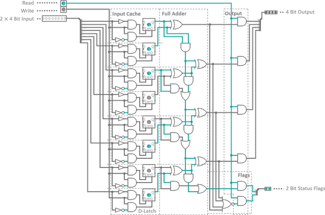
It might have caught your attention, that besides the already mentioned components there is one more functional block added to the instruction called Flags. A flag is a single bit indicator displaying the status of a specific operation parameter. In case of our ADD instruction the two flags are CF (carry flag), indicating that the result exceeded the 4‑bit data width and overflowed into the fifth bit, and ZF (zero flag), which is active when none of the output bits are high i.e. the operation yields zero (excluding the carry bit). The latter is implemented by putting all four output bits into a NOR gate. A logic gate with more than two inputs can always be constructed by stacking a pyramid of regular two input gates behind each other. With every consecutive pyramid level the number of inputs is reduced by one, until no unpaired inputs are left (see figure 9). The flags will later be used to control conditional instructions (as in, do something when this flag is active).

This is the first - and most probably only - arithmetic instruction our processor will have. Therefore, apart from a simple logic compare instruction, our Arithmetic-Logic-Unit (ALU) is 50% complete. On our overall road map for a complete processor that amounts to 67 components placed, 834 more to go... so, a little work still lies ahead of us.
Nevertheless, we have set sail on our journey towards a finished processor unit for good this time. In the next part, we will have a look at registers and decoders. Stay tuned.
[1] Wolfram Alpha's Boolean Algebra Calculator (widget)
[2] Logisim, Logic Simulator (download)
Congratulations, you were selected for a random upvote! Follow @resteemy and upvote this post to increase your chance of being upvoted again!
Read more about @resteemy here.