Intel and GlobalFoundries talked about the benefits of their new manufacturing processes

Intel and GlobalFoundries talked about the benefits of their new manufacturing processes
During the IEEE International Electron Device Meeting (IEDM) event in San Francisco, chip manufacturers talked about what technological solutions they would soon begin to use to release their products.
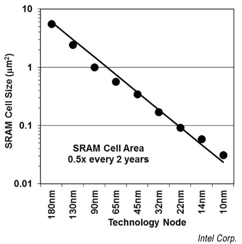
Intel researchers presented a 10-nanometer technology platform and stated that it provides superior transistor and interconnect performance, as well as excellent design scalability. Also, the platform was demonstrated in the form of a 204 MB SRAM chip, which includes three different types of memory cells: high-density cells with an area of 0.0312 μm2, cells with low energy consumption of 0.0367 μm2 area, high-performance cells with an area of 0.0441 μm2.
The platform provides for the use of production technology FinFET the third generation with the use of SAQP for critical layers (self-aligned quadruple patterning), which provides a plate width of 7 nm at 34 nm and a plate height of 46 nm; High-k technology of the fifth generation; the technology of extended silicon of the seventh generation. It is also noted that Intel uses cobalt in the two lower layers of interconnects within the 10-nanometer process technology. Thanks to the introduction of cobalt, it was possible to improve the situation by 5-10 times electromigration and to reduce the resistance by half. All these innovations allowed to increase the current of NMOS and PMOS by 71% and 35%, respectively, in comparison with 14-nanometer production technology FinFET.

In turn, the company GlobalFoundries said that within the 7-nanometer production technology, it will continue to use a combination of copper and High-k dielectrics, as in previous technologies. This will provide a number of advantages, such as high reliability, less complexity and higher yield rates. The researchers also presented a fully integrated 7-nanometer CMOS platform, which provides significant scalability of component density and improved performance compared to the 14-nanometer production technology. Within this platform, the third-generation FinFET technology with SAQP (self-aligned quadruple patterning) for plate formation and SADP (self-aligned double patterning for metallization) for metallization is used.
At the same time, the company said that the technology platform was developed with the possibility of using the advantages of EUV lithography for certain levels with several templates. This will improve production efficiency. At the same time, GlobalFoundries states that some EUV-lithography parameters still need to be improved. Nevertheless, the company has already begun to install the appropriate production equipment for EUV lithography at its Fab 8 factory in New York State.
GlobalFoundries notes that the 7-nanometer production platform provides a 2.8-fold advantage in wiring density compared to 14-nanometer manufacturing technology. It also claims a performance increase with an unchanged energy consumption of more than 40% or a decrease in power consumption by 55% at a constant frequency.
In addition, it is reported that GlobalFoundries offers a full set of the necessary basis and intellectual property within its improved CMOS production platform. It will allow creating high-performance computer and mobile solutions.
Although Intel and GlobalFoundries did not provide detailed technical details, improvements in the density of transistors in comparison with the previous generation are almost in line with Moore's law.
Source: cdrinfo

Thanks for the tech update! Always find this stuff interesting! If you check out my blog and find it of interest to you, please follow me as I have you.
thanks for check, cya
Its the great milestone that we heard from Intel that then new platform(7 nano) gives the better energy efficiency than 14, 2.8 times. Great news from you.. @kobusu
Quite detailed and Informative. You a scientist brother? :D
Thank bro, nah. Not a big deal publish known data :)
This post has received a 1.52 % upvote from @buildawhale thanks to: @kobusu. Send at least 1 SBD to @buildawhale with a post link in the memo field for a portion of the next vote.
To support our daily curation initiative, please vote on my owner, @themarkymark, as a Steem Witness
This post has received gratitude of 1.64 % from @appreciator thanks to: @kobusu.
@originalworks
The @OriginalWorks bot has determined this post by @kobusu to be original material and upvoted(1.5%) it!
To call @OriginalWorks, simply reply to any post with @originalworks or !originalworks in your message!