Lattice 2D Materials and Spintronics: Towards Ending Obsolescence in Electronics
One of the paradigms of the current state of the art in computer science regarding artificial intelligence is that machines are stupid (sorry, dear PC) in order for them to thrive we need to make the environment smart for them. Well, that's what we humans have been doing for us, since the birth of thought.
We store information in the form of electrons in a particular state. Every electron has mass, charge, and spin. So far for most of our current electronics, we only use two of the properties: Mass and charge.
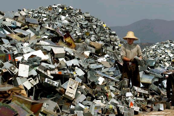
As you might imagine this means we are highly inefficient, this is the reason we generate so much heat in order to increase computational power. Also, the reason we create so much waste in the process. You could see it as a point for optimization. Isn't it optimizing cleaning the place so the dumb doesn't get hurt?
The spin acts like a mini bar magnet but one that is an up and down state. Normally to use this property we need perfect materials or imperfect materials. Sounds counter intuitive or redundant, yeah, most things in science do.
Thanks to explorations of the physical limits of silicon transistors and circuits.[1]
Predictions of the rate of advancement have been advancing steadily. Things have not changed much since the early days when the first predictions were made. [2]
By the laws of thermodynamics, it seems unlikely we'll be able to continue growing the storage of information and processing power beyond the scope of the atomic level. By 2020 we are bound to run into some troubles at advancing the logarithmic growth we have at the moment.
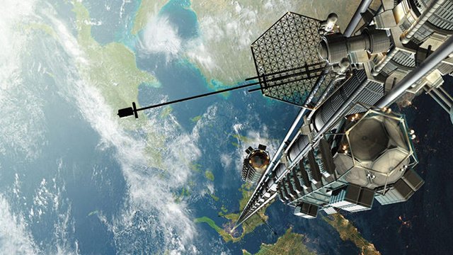
Have you heard of graphene? Of course you have! Is like the promised manna of the chemical material sciences. That will bring us with cables made of nanotubes into space. Single atoms of carbon in a single plane array.
Most of the materials like graphene were already theorized decades ago. The absolute brilliance of taking a scotch tape and some graphite to check for the flakes of graphene on an electrons microscope is so simple and so magnificent at the same time. The exfoliation method.3
2D crystals behave like semimetals. Have potential utility for electronics as they allow travel of electrons long distances with minimum scattering to no scattering. While traveling in the mesh electrons behave like they have no mass.
Mass production of 2d materials of high quality is still far off in the future. I tried to get some myself, graphene is at the moment close to $25 the gram for >80% pure flakes of 3-4nm. I might have to wait a little more.

Is like playing with atomic legos. The first one to do this was IBM back in 1989.
They printed with just a couple of legos their logo. They were not connected, but still is the first recorded modern alchemy of these materials.

source
A relative easier alternative would be to use diamonds. Yes, diamonds. The weird world where diamonds are cheaper than graphene is here. Remember Superman comics? their civilization used crystals as the basis of their technology. We may be heading that way. 4
 .
.
Source
When a diamond has imperfections, missing atoms of carbon in the mesh structure behave like an electron trap thanks to the nitrogen impurities. This allows us to determine with high precision the direction of the spin by using light at a particular wavelength. Read the spin one at a time, or change the spin. Or get a magnet to whip the spin. Like directing a ballerina.

We could store information actively at the atomic level. Even redefining the nature of information itself. No more junk electronics in the trash. We could have a single crystal device the size of a phone with the computational power of the entire world as we know it.

source
For instance one of the seminal works is the article by Mak et al on how we could control the direction of spin in a lattice of molybdenum disulfide. 5 That would allow for us to explore nature from the atomic scale to the galactic scale.
The fields of physics dealing with properties of these materials are:
- Quantum Transport
- Spintronics
- Optoelectronics
The first place you will see this material into daily life is gonna be your tennis racket. If you are a tennis player. Otherwise is your smartphone.
If semiconductors are the network of the digital brain then what if the same properties could make your own body lighter, more nimble and even invisible. Human and machine could actually become one.
[1] Robert W Keyes; Physical limits of silicon transistors and circuits; Reports on Progress in Physics, Volume 68, Number 12 2005
[2] R. W. Keyes. Miniaturization of electronics and its limits. IBM Journal of Research and Development ( Volume: 32, Issue: 1, Jan. 1988)
[3] Andrey Geim, Allan MacDonald. Graphene: Exploring carbon flatland: Just one atom thick, this two-dimensional semiconductor does not resemble any known material. Physics Today 60, 8, 35 (2007)
[4] https://www.wired.com/2003/09/diamond/
[5] Kin Fai Mak et al; Control of valley polarization in monolayer MoS2 by optical helicity. Nature Nanotechnology 7, 494–498 (2012)

This post has received a 2.87 % upvote from @buildawhale thanks to: @trumpman. Send 0.100 or more SBD to @buildawhale with a post link in the memo field to bid on the next vote.
To support our curation initiative, please vote on my owner, @themarkymark, as a Steem Witness