Shift Register

| I. Intended Learning Objectives |
|---|
| At the end of the tutorial, the readers should be able to: 1. Explain the operation of a shift register 2. Construct the digital circuit using CircuitSim for a shift register; and, 3. Perform simulation of the operation of a shift register. |
| II. Requirements |
|---|
| The readers should have a desktop PC or laptop (Win 7, 8, or 10) with an installed CircuitSim simulator to be able to effectively learn the concepts and procedures that will be discussed in this tutorial. Readers will be able to download a copy of the app at ra4king.github.io/CircuitSim/ download page or visit its official Github repository at ra4king/CircuitSim. |
| III. Difficulty |
|---|
| Intermediate |
| IV. Introduction to Shift Register |
|---|
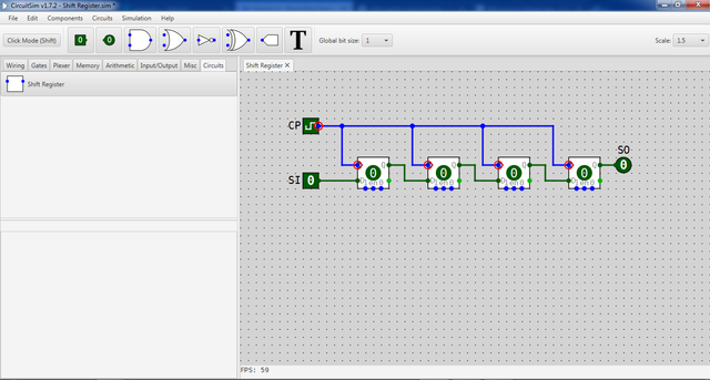
| Basically, a register capable of shifting the binary information either to the right or to the left is called a shift register. Shift Register is configure with cascaded flip-flops where the output of one flip-flop is connected to the succeeding flip-flop. At the same time, all flip-flops receive a uniform clock pulse that cause the shift from one stage to the next. The simplest possible shift register is constructed using flip-flops. The Q output of each flip-flop is connected to the D input of the succeeding flip-flop to its right. Each clock pulse shifts the contents of the register one bit position to the right. Table 1: Operation of Shift-right Register The serial input determine rightmost flip-flop prior the application of a clock pulse. For example, serial input for QA, from the table 1, is 0, a shift of logic value is pass through QB and so on, until it reach the rightmost flip-flop. A way to control the shifting operation is to set a predetermined clock pulse. For the this, tutorial, we will be implementing a shift-right register using a cascaded four set of D Flip-Flop. In addition, we will implement a serial transfer application of the shift register that we will be creating. |
| VI. Simulation of the Shift Register |
|---|
We have now created the a shift register. To start the simulation, simply click simulation > simulation enable and also clock enable. In the running simulation as shown, we can observe a different bit value in each D Flip-Flop. This values changes state in sequence and in accordance to the clock pulse. The shifting of values terminates at it reaches the final and the rightmost D Flip-Flop.The shift register simulation can be seen on the video below.Simulation 1: Shift RegisterIn addition, we constructed the a circuit that we are able to control the shift of the bit values in a shift registry by adding an AND gate that enables only the logic 1 of the clock pulse. The full simulation of the circuit is shown below. Simulation 2: Shift Register with clock pulse controlYou can observe that there is a time required before we get a logic 1 output in the second simulation. This means that the simulation run first the shifts inside in each shift register. The operation and behavior undergone by the time lapse in the second simulation is equivocal to the operation presented in the first simulation. |
| VII. Summary |
|---|
| In this tutorial, we start by understanding the operation of a shift register. So, we learn that a shift register operates in a way that the serial input is shifted from leftmost flip-flop and store the shifted value on the flip-flop. The circuit is made of a cascaded four set of D Flip-Flop arrange horizontally from left to right. The leftmost D Flip-Flop receives the serial input and shifted it to another bit to the succeeding D Flip-Flop. The D Flip-Flop is connected with a common clock pulse. In addition, we constructed the a circuit that we are able to control the shift of the bit values in a shift registry by adding an AND gate that enables only the logic 1 of the clock pulse. All stated circuit config is presented in two sets of simulation to clearly elaborate how it works. |
| VIII. Reference |
|---|
| Conceptual Reference: Morris Mano, Digital Design, 3rd Edition Image and Video Source: All videos and images use in this tutorial is recorded and captured by the author. Otherwise, it is specified in the text. |
| IX. Curriculum |
|---|
| You can browse my other tutorial for digital circuits implemented using CircuitSim from the following links bellow. 1. Binary Ripple Counter |
Posted on Utopian.io - Rewarding Open Source Contributors


Thank you for the contribution. It has been approved.
Are you using tables to construct your posts? That would explain the very dense format you are using. I think breaks cannot be build into tables.
You can contact us on Discord.
[utopian-moderator]
Hey @flauwy, I just gave you a tip for your hard work on moderation. Upvote this comment to support the utopian moderators and increase your future rewards!
Yes, I am using tables to create highlights on headers. I try to consider another formating technique. Thank you , @flauwy!
Hey @juecoree I am @utopian-io. I have just upvoted you!
Achievements
Community-Driven Witness!
I am the first and only Steem Community-Driven Witness. Participate on Discord. Lets GROW TOGETHER!
Up-vote this comment to grow my power and help Open Source contributions like this one. Want to chat? Join me on Discord https://discord.gg/Pc8HG9x
Resteemed your article. This article was resteemed because you are part of the New Steemians project. You can learn more about it here: https://steemit.com/introduceyourself/@gaman/new-steemians-project-launch . If your post has more upvotes, your post will appear in the trending page. To get more upvotes, you can bid for @steembidbot vote. please check it out here: https://steembottracker.com/