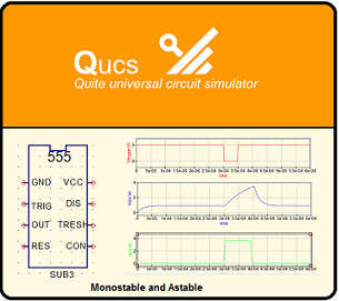
Qucs simulator tools, to analyze the monostable and astable multivibrator.
What Will I Learn?
In this tutorial you will learn:
Develop the analysis functions of the Qucs, for monostable and astable mutivibrators.
Know the tools of the Qucs for the modeling of integrated circuits.
Learn to extract the netlist code from the subcircuits designed in the Qucs.
Requirements
Use the tools of the Qucs Simulator.
work with subcircuits in the Qucs .
Know the internal design 555 integrated circuit.
Know the design of monostable and astable multivibrators with the 555.
Difficulty
- Intermediate
Tutorial Contents
The following tutorial is a contribution of the @edagmi account for utopian-io. The functions of the Qucs Simulator are presented, to analyze integrated circuits of specific applications, the case study will be with the 555 integrated circuit, to simulate its most useful applications. It is important to note that the tutorial is focused on demonstrating the potential of the Qucs for the analysis of two important applications of the 555 for the generation of pulse signals:
- Monostable multivibrator or timer.
- Astable multivibrator or the pulse generator.
The Qucs does not have the integrated circuit 555 in its libraries, so it is required to do a modeling of it, based on a series of analog and digital circuits that emulate the real behavior of the IC 555. The tutorial shows the utility of the simulator for applications with the 555 and does not focus on the internal design of the 555 circuit. Two fundamental applications of the 555 are referenced and then the functionality of the Qucs for the simulation is demonstrated.
Below is a series of steps to develop the tutorial, I hope it will be very useful.
Step 1:
Select CI 555 in the Qucs. CI 555 is not found directly in any of the Qucs libraries, so reference is made to a model created on the official Qucs website (http://qucs.sourceforge.net/examples.html ), with subcircuits necessary to completely model their behavior. The following image shows the subcircuit of 555 in the Qucs.

Step 2:
Identify the connection terminals of the CI 555. The encapsulation has 8 pins, with the following relevant characteristics:
- Ground.
- Input signal (Trigger).
- Output signal Pulses generated.
- Threshold (Comparison voltage for astable function).
- Download (To download capacitor).
- Alimentation.
The Qucs allows connecting different schematic circuits, through functions known as subcircuits. The following image shows the 555 model, which responds to a combination of digital and analog subcircuits designed in the Qucs, which define the operation of each of the 555 pins. In this tutorial the internal design of the 555 is not described. 555 integrated circuit, the functions of the different subcircuits that compose them are not analyzed either.

Step 3:
Observe the netlist created for the CI 555 model. The netlist is the description of the connectivity of an electronic circuit, it is a list of components identified by nodes, which define the connection points of the components of the circuit, in a universal language for the electronic simulators. You can see the 555 netlist by selecting the circuit and copying it into the text editor that presents the Qucs in its main menu.

Netlist code of 555:
<Components>
<Port P_GND 1 820 300 4 12 1 2 "1" 0 "analog" 0>
<Port P_OUTPUT 1 820 230 4 -28 0 2 "3" 0 "analog" 0>
<R R1 1 220 100 15 -26 0 1 "5k" 1 "26.85" 0 "0.0" 0 "0.0" 0 "26.85" 0 "european" 0>
<Port P_RESET 1 150 40 -23 12 0 0 "4" 0 "analog" 0>
<R R2 1 220 250 15 -26 0 1 "5k" 1 "26.85" 0 "0.0" 0 "0.0" 0 "26.85" 0 "european" 0>
<R R3 1 220 400 15 -26 0 1 "5k" 1 "26.85" 0 "0.0" 0 "0.0" 0 "26.85" 0 "european" 0>
<Port P_CONTROL 1 150 200 -23 12 0 0 "5" 0 "analog" 0>
<Port P_DISCHARGE 1 820 360 4 12 1 2 "7" 0 "analog" 0>
<Port P_VCC 1 220 30 -54 -23 0 3 "8" 0 "analog" 0>
<Port P_TRIGGER 1 140 355 -23 12 0 0 "2" 0 "analog" 0>
<Port P_THRESH 1 120 140 -23 12 0 0 "6" 0 "analog" 0>
<Sub SUB5 1 660 390 -50 104 0 0 "timer_Discharge.sch" 0>
<Sub SUB6 1 305 320 5 39 0 0 "timer_trig.sch" 1>
<Sub SUB7 1 285 170 5 49 0 0 "timer_thresh.sch" 1>
<Sub SUB3 1 535 200 -15 74 0 0 "timer_digital_comb.sch" 0>
<Sub SUB4 1 730 230 -20 99 0 0 "timer_amp.sch" 0>
</Components>
<Wires>
<690 260 690 300 "" 0 0 0 "">
<690 300 760 300 "" 0 0 0 "">
<760 300 820 300 "" 0 0 0 "">
<760 300 760 480 "" 0 0 0 "">
<220 280 220 300 "" 0 0 0 "">
<220 130 220 200 "" 0 0 0 "">
<220 200 220 220 "" 0 0 0 "">
<150 200 220 200 "" 0 0 0 "">
<220 30 220 70 "" 0 0 0 "">
<220 430 560 430 "" 0 0 0 "">
<560 300 560 430 "" 0 0 0 "">
<560 300 690 300 "" 0 0 0 "">
<505 40 505 200 "" 0 0 0 "">
<150 40 505 40 "" 0 0 0 "">
<585 200 690 200 "" 0 0 0 "">
<585 410 610 410 "" 0 0 0 "">
<585 240 585 410 "" 0 0 0 "">
<710 360 820 360 "" 0 0 0 "">
<670 470 670 480 "" 0 0 0 "">
<670 480 760 480 "" 0 0 0 "">
<275 280 275 300 "" 0 0 0 "">
<220 300 220 370 "" 0 0 0 "">
<220 300 275 300 "" 0 0 0 "">
<140 350 275 350 "" 0 0 0 "">
<140 350 140 355 "" 0 0 0 "">
<385 315 505 315 "" 0 0 0 "">
<505 240 505 315 "" 0 0 0 "">
<120 140 255 140 "" 0 0 0 "">
<220 200 255 200 "" 0 0 0 "">
<375 170 375 220 "" 0 0 0 "">
<375 220 505 220 "" 0 0 0 "">
</Wires>
<Diagrams>
</Diagrams>
<Paintings>
</Paintings>
Step 4:
Build in the schematic diagram of the Qucs, the monostable timer circuit using the 555, for this one requires a resistor, two capacitors, power supply, ground connection and a pulse for the trigger signal. All the elements are extracted from the component menu of the program. Observe in the following image:
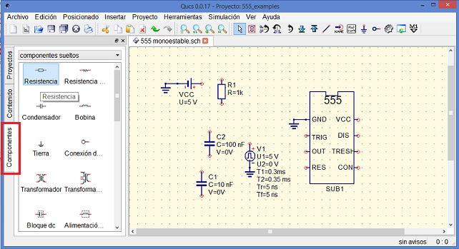
Step 5:
The connection of the monostable circuit is made, as shown in the image below, and it is also subjected to a transient analysis as a function of time, in order to see the most relevant signals of the circuit.

Step 6:
The simulated application with the Qucs, must show a pulse generated by the 555, due to the trigger signal. The pulse has a width that can be controlled with the resistive element of the circuit and is given by the following equation:
T = 1.1 * R1 * C2
For the case study, a pulse width of approximately 110 μsec is given.
Step 7:
The simulation shows three Cartesian graphs, the first graph shows the trigger pulse (Vtrigger), the second graph shows the capacitor charge process (Vdis) and in the third graph the output pulse is observed with a width controlled and close to the 110 μsec (Vout).

Step 8:
The netlist of the monostable 555 circuit can be observed.
<Components>
<Sub SUB1 1 490 300 0 104 0 0 "timer_555.sch" 0>
<GND * 1 610 420 0 0 0 0>
<GND * 1 410 240 0 0 0 0>
<GND * 1 90 150 0 0 0 0>
<Vdc VCC 1 150 150 -26 18 0 0 "5 V" 1>
<Vpulse V1 1 300 330 18 -26 0 1 "5 V" 1 "0 V" 1 "0.3ms" 1 "0.35 ms" 1 "5 ns" 1 "5 ns" 1>
<GND * 1 300 360 0 0 0 0>
<C C1 1 610 390 17 -26 0 1 "10 nF" 1 "0V" 1 "neutral" 0>
<R R1 1 200 240 15 -26 0 1 "1k" 1 "26.85" 0 "0.0" 0 "0.0" 0 "26.85" 0 "european" 0>
<C C2 1 200 300 17 -26 0 1 "100 nF" 1 "0V" 1 "neutral" 0>
<GND * 1 200 330 0 0 0 0>
<.TR TR1 1 690 110 0 77 0 0 "lin" 1 "0" 1 "0.6 ms" 1 "201" 1 "Gear" 1 "6" 1 "1 ns" 0 "1e-16" 0 "150" 0 "0.001" 0 "1 pA" 0 "1 uV" 0 "26.85" 0 "1e-3" 0 "1e-6" 0 "1" 0 "CroutLU" 0 "no" 0 "yes" 0 "0" 0>
</Components>
<Wires>
<570 360 610 360 "" 0 0 0 "">
<180 150 200 150 "" 0 0 0 "">
<600 150 600 240 "" 0 0 0 "">
<570 240 600 240 "" 0 0 0 "">
<570 280 600 280 "" 0 0 0 "">
<570 320 600 320 "" 0 0 0 "">
<600 280 600 320 "" 0 0 0 "">
<410 240 440 240 "" 0 0 0 "">
<90 150 120 150 "" 0 0 0 "">
<200 150 390 150 "" 0 0 0 "">
<200 150 200 210 "" 0 0 0 "">
<300 280 440 280 "" 0 0 0 "">
<300 280 300 300 "" 0 0 0 "">
<410 360 440 360 "" 0 0 0 "">
<410 330 410 360 "" 0 0 0 "">
<390 330 410 330 "" 0 0 0 "">
<390 150 600 150 "" 0 0 0 "">
<390 150 390 330 "" 0 0 0 "">
<600 320 600 340 "" 0 0 0 "">
<580 340 600 340 "" 0 0 0 "">
<580 340 580 440 "" 0 0 0 "">
<160 440 580 440 "" 0 0 0 "">
<160 270 160 440 "" 0 0 0 "">
<160 270 200 270 "" 0 0 0 "">
<440 320 440 320 "vout" 400 290 0 "">
<600 320 600 320 "Vdis" 630 290 0 "">
<300 280 300 280 "Vtrigger" 330 250 0 "">
</Wires>
<Diagrams>
</Diagrams>
<Paintings>
</Paintings>
Step 9:
Following the same sequence of steps 4 and 5, we proceed to arm the astable circuit with the 555 and again perform a transient analysis, as seen in the following image.

Step 10:
For the second simulation of the Qucs, it is expected that a train of pulses will be generated at the output, where the capacitor C1 is permanently charging and discharging. When the capacitor is charging the output of the IC 555 is at high level (5V) and when the capacitor is discharging the output of the IC 555 is at low level (0V). The time that is at high level can be calculated with the following equation:
T = 0.7 * (R1+R2) * C2
The time that is at low level (0V) can be calculated with the following equation:
T = 0.7 * R2 * C2
Step 11:
The responses of the transient simulation of the Qucs are verified, for the following signals:
- Reset signal used to activate the astable (Reset).
- The trigger signals (Vtrigger).
- The capacitor discharge (Vdis).
- The pulse train output signal generated by the circuit (Vout). Observe the data obtained from these transitory responses in the following image.

Step 12:
You can see the astable 555 circuit netlist:
<Components>
<Sub SUB1 1 530 280 0 104 0 0 "timer_555.sch" 0>
<GND * 1 650 400 0 0 0 0>
<GND * 1 450 220 0 0 0 0>
<GND * 1 220 430 0 0 0 0>
<Vpulse V1 1 400 370 18 -26 0 1 "5 V" 1 "0 V" 1 "0" 1 "0.02 ms" 1 "5 ns" 1 "5 ns" 1>
<GND * 1 400 400 0 0 0 0>
<GND * 1 120 130 0 0 0 0>
<Vdc VCC 1 170 130 -26 18 0 0 "5 V" 1>
<.TR TR1 1 790 90 0 77 0 0 "lin" 1 "0" 1 "0.9 ms" 1 "90" 1 "Gear" 1 "6" 1 "1 ns" 0 "1e-16" 0 "1500" 1 "0.01" 1 "100 pA" 1 "100 uV" 1 "26.85" 0 "1e-3" 0 "1e-6" 0 "1" 0 "CroutLU" 0 "no" 0 "yes" 0 "0" 0>
<C C1 1 650 370 17 -26 0 1 "10 nF" 1 "0V" 1 "neutral" 0>
<C C2 1 220 400 17 -26 0 1 "50 nF" 1 "0V" 1 "neutral" 0>
<R R1 1 220 200 15 -26 0 1 "3.2k" 1 "26.85" 0 "0.0" 0 "0.0" 0 "26.85" 0 "european" 0>
<R R2 1 220 310 15 -26 0 1 "2k" 1 "26.85" 0 "0.0" 0 "0.0" 0 "26.85" 0 "european" 0>
</Components>
<Wires>
<610 340 650 340 "" 0 0 0 "">
<220 130 220 170 "" 0 0 0 "">
<220 130 640 130 "" 0 0 0 "">
<640 130 640 220 "" 0 0 0 "">
<610 220 640 220 "" 0 0 0 "">
<220 230 220 260 "" 0 0 0 "">
<450 220 480 220 "" 0 0 0 "">
<350 260 480 260 "" 0 0 0 "">
<220 260 320 260 "" 0 0 0 "">
<610 260 750 260 "Vdis" 690 230 46 "">
<220 260 220 280 "" 0 0 0 "">
<220 340 220 360 "" 0 0 0 "">
<220 360 220 370 "" 0 0 0 "">
<220 360 350 360 "" 0 0 0 "">
<350 260 350 360 "" 0 0 0 "">
<400 340 480 340 "" 0 0 0 "">
<610 300 630 300 "" 0 0 0 "">
<630 300 630 510 "" 0 0 0 "">
<350 360 350 510 "" 0 0 0 "">
<350 510 630 510 "" 0 0 0 "">
<320 260 320 520 "" 0 0 0 "">
<320 520 750 520 "" 0 0 0 "">
<750 260 750 520 "" 0 0 0 "">
<200 130 220 130 "" 0 0 0 "">
<120 130 140 130 "" 0 0 0 "">
<480 300 480 300 "Vout" 436 270 0 "">
<350 260 350 260 "Vtrigger" 370 210 0 "">
<400 340 400 340 "Reset" 430 310 0 "">
</Wires>
<Diagrams>
</Diagrams>
<Paintings>
</Paintings>
Thanks for your attention.
Curriculum
- Qucs simulator for semiconductor electronic circuits: Introduction
- Stages of design of a source regulated with Zener, using QUCS.
- Design of an amplifier of audio with Qucs
Posted on Utopian.io - Rewarding Open Source Contributors
Unfortunately, I have to reject your contribution due to an update on the rules.
We do not accept circuit design tutorials anymore.
Need help? Write a ticket on https://support.utopian.io.
Chat with us on Discord.
[utopian-moderator]
Congratulations! This post has been upvoted from the communal account, @minnowsupport, by edagmi from the Minnow Support Project. It's a witness project run by aggroed, ausbitbank, teamsteem, theprophet0, someguy123, neoxian, followbtcnews, and netuoso. The goal is to help Steemit grow by supporting Minnows. Please find us at the Peace, Abundance, and Liberty Network (PALnet) Discord Channel. It's a completely public and open space to all members of the Steemit community who voluntarily choose to be there.
If you would like to delegate to the Minnow Support Project you can do so by clicking on the following links: 50SP, 100SP, 250SP, 500SP, 1000SP, 5000SP.
Be sure to leave at least 50SP undelegated on your account.