Design of a door opening system, with MOSFET transistors and with CMOS logic, using the QUCS.
What Will I Learn?
In this tutorial you will learn:
Work with digital signals
Use the MOSFET transistor to design digital gates.
Use the Qucs for the design of control systems based on digital gates.
Know the CMOS logic.
Requirements
Advanced knowledge of electronic devices
Analysis of combinational logic of digital gates.
Use the Qucs simulator for digital signals.
Difficulty
- Advanced
Tutorial Contents
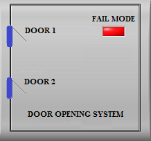
Greetings community Utopian-io, the following tutorial of the account @edagmi, is a material used in the career of electronic engineering in Venezuela. This material corresponds to the design of a door opening system, with two doors that has the following working condition: In Normal mode the doors must be open or closed at the same time, in Fail mode the doors lose synchronicity, that is to say a open and the other closed, in this mode the system must activate a visual alarm. The system must be realized with logic gates designed with MOSFETS transistors, using Complementary CMOS logic. The QUCS is used to simulate the electronic circuits of the design.
The circuits used to design logic gates in digital electronics, are based on polarized transistors to work in their regions of cut and saturation, depending on the type of transistor used for the design of gates, you can talk about a TTL logic, for the case of BJT transistors or a CMOS logic, for FETs field effect transistors.
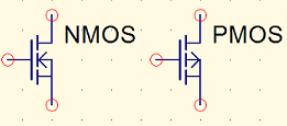
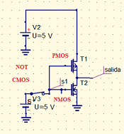
The FETs have a family of transistors that use a metal-oxide-semiconductor junction, which defines it as a MOSFET transistor. These are classified in MOSFET type D and type E. MOSFET type E is classified in NMOS and PMOS, This classification is due to the type of semiconductor material that is used for its manufacture. When NMOS and PMOS are used in pairs, to design gates they are defined as complementary MOS or CMOS.
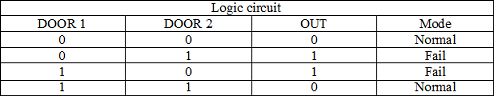
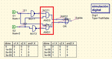
The logic is observed in the following table, corresponds to the logic of an Exclusive OR gate or XOR.
The XOR gate can be designed in the QUCS by combining another type of gate, in this case NOT, AND and OR gates.
The design requires an Exclusive OR gate, using CMOS logic with the MOSFET type E transistors. Next we will describe a series of steps to achieve the required design, using the Qucs electronic circuit simulator.
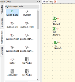
Step 1:
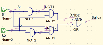
Select the digital components to design the XOR gate. In the QUCS library, all the components of the circuit are found. For this case we will use two inverter gates, two AND gates, one OR gates, and digital input signals.
Step 2:
Complete the circuit formed by the digital gates with their respective labels corresponding to the input and output signals. We proceed to select the digital simulation to generate the truth table.
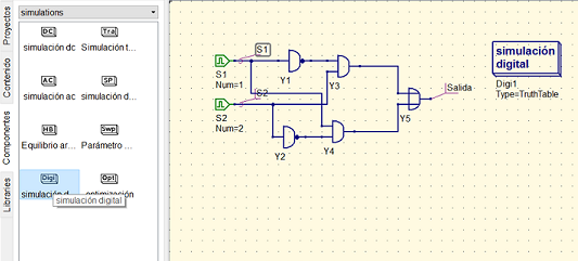
Step 3:
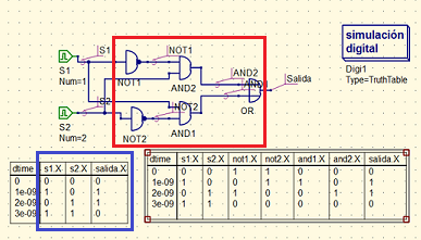
The simulation is executed and the truth tables are selected, in order to visualize the data. The parameters shown in the table for our case are S1 and S2 as the circuit input switches and the output is the activation of the Fail mode.
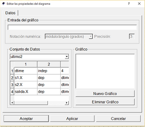
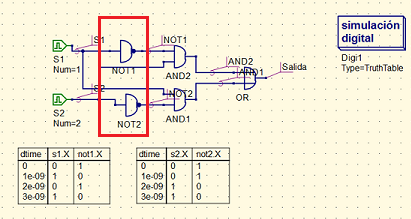
Step 4:
The truth table of the gates that make up the design is displayed. The input signals are tracked. The NOT gates of the digital circuit are displayed first.
Step 5:
Proceed to visualize the AND gates of the digital circuit.
Step 6:
The complete logic of the circuit including the OR gate is visualized and it is verified that the circuit complies with the logic of the XOR gate, the logic corresponds with the desired solution in the design of the door opening system.
Step 7:
Now proceed to design each of the gates, using the MOSFET transistors, located in the list of non-linear components of the QUCS.
Step 8:
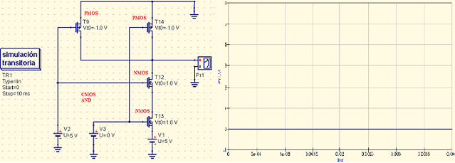
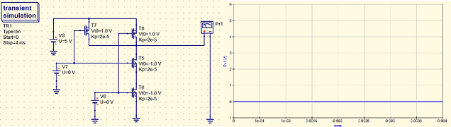
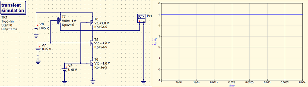
We design two NOT CMOS gates, each with a pair of PMOS and NMOS transistors in complementary mode, that is, equal number of N channel and P channel transistors.
Step 9:
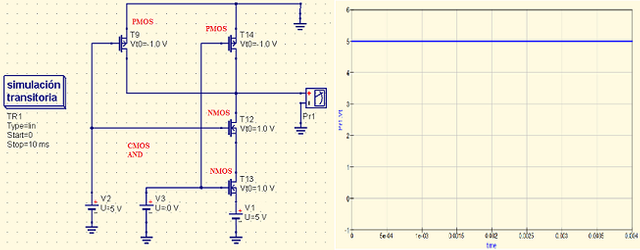
We design two AND CMOS gates, and we can test them to see the logical response for high and low voltage input signals.
Step 10:
We design two OR CMOS gates, and we can test them to see the logical response for high and low voltage input signals.
Step 11:
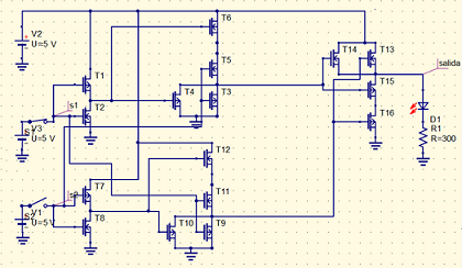
We connect all the stages to get the XOR gate, which corresponds to the resulting combinatorial logic to activate the failure mode of our access control circuit. A Led diode is added to the output signal that serves as an activation alarm for the Fail mode.
Thank you for your attention we will see you in the next tutorial.
Curriculum
- Qucs simulator for semiconductor electronic circuits: Introduction
- Stages of design of a source regulated with Zener, using QUCS.
- Design of an amplifier of audio with Qucs
Posted on Utopian.io - Rewarding Open Source Contributors
Your contribution cannot be approved because it does not follow the Utopian Rules.
You can contact us on Discord.
[utopian-moderator]