Design and Analysis of an operational amplifier with BJT transistors, using the Qucs simulator.
What Will I Learn?
In this tutorial you will learn:
Work with operational amplifiers
Use the BJT transistor to design differential amplifiers and current sources.
Use the Qucs for the design and analysis of real models of electronic devices.
Requirements
Advanced knowledge of electronic devices
Analysis of amplifiers with BJT transistors.
Design of current mirrors
Use the Qucs simulator for transient analis, DC, AC and parametric sweep.
Difficulty
- Advanced
Tutorial Contents
Greetings community Utopian-io, the following tutorial of the account @edagmi, is a material used in the career of electronic engineering in Venezuela. In this tutorial tutorial the model of the real operational amplifier is designed and analyzed, it is visualized as an electronic device built with a series of amplifiers and current sources designed with BJT bipolar transistors, very useful in electronics as an ideal amplifier for alternate signals and polarized with continuous sources.
We will work with a real model of the operational amplifier, to proceed to assemble and analyze it in the Qucs electronic simulation program. The model is subjected to different types of analysis to verify its response. The following figure shows the stages that make up the operational amplifier.
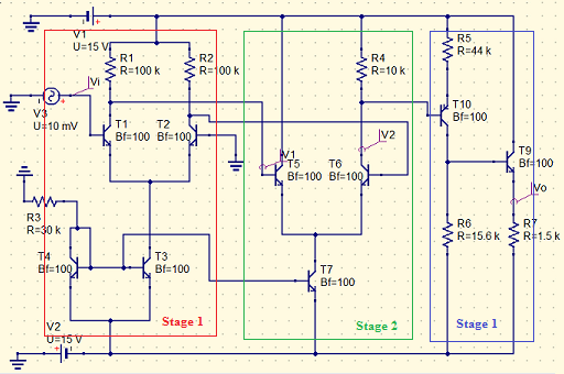
Stage I:
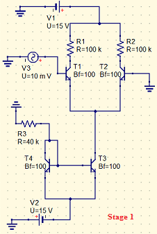
This consists of the bipolar differential amplifier known as pair coupled by emitter. This circuit forms the input of many operational amplifiers and comparators. In the pair coupled by the emitter, it is assumed that the transistors are equal (T1 and T2). The amplified output voltage is given by the following equation:
Vo=Rc(ic2-ic1)
There is also a current source called a current mirror, which is responsible for polarizing the amplifier of the coupled pair. In the current source the transistors (T3 and T4) are equal, in addition this current mirror contains a dynamic resistance (R3), which changes the bias current of the coupled pair. The current flowing through R3 is called reference current Iref which is given by:
I_ref=(Vcc-VBE)/R
Design of the first stage with BJT NPN transistors, using the Qucs simulator.
Stage II:
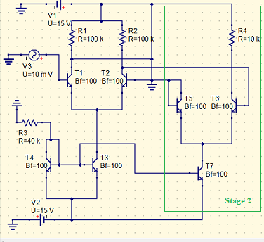
The direct coupling to the differential input of the second stage is implemented, which operates in the same way as stage I, described above. In this case, transistor T7, biases the differential amplifier given by transistors T5 and T6. In the following image stage 2 is added to stage 1.
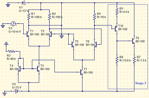
Stage III:
It is formed by a current amplifier with a pair of complementary transistors, with a follower emitter configuration that establishes a low output impedance of the operational amplifier. In the following image the circuit with the three stages of the real operational amplifier is observed.
After designing the operational amplifier with the real model, we proceed to perform the different analyzes that define the characteristic responses of the device.
Transient Analysis
First a Transient analysis will be performed to see the responses of the amplification stages:
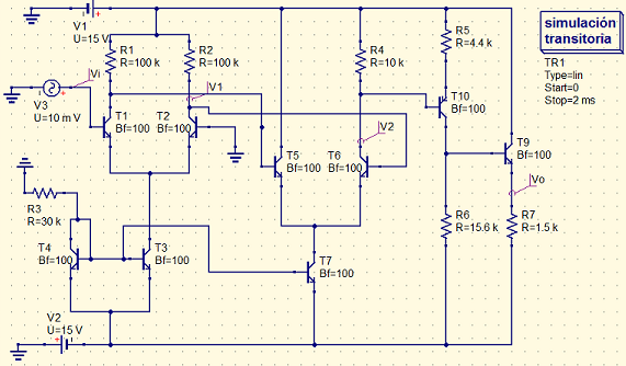
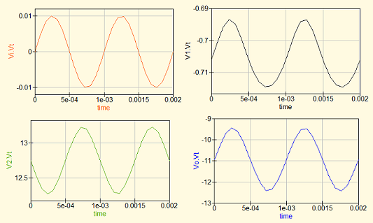
In the transient analysis we use four nodes to verify the output, Vi for the input signal, V1 for the output of the first amplifier, V2 for the output of the second amplifier and Vo for the output of the operational amplifier. The following graph shows the response as a function of time of the four outputs, for an input signal of 10 mV at 1KHz frequency.
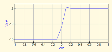
DC Analysis
Second, a DC analysis is performed, with a parametric sweep of the input signal of the first amplifier, based on its output voltage to see the linear operating range of the amplifier.
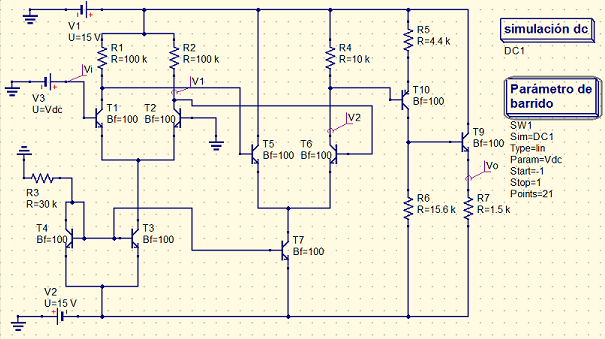
The parametric sweep is done for a DC voltage source at the amplifier input, for a range of -1 to 1 V.
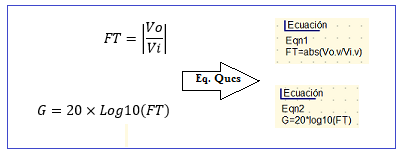
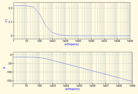
AC Analysis
Finally, an AC analysis is performed to determine the frequency response of the amplifier. To verify the gain factor, the equation editor of the Qucs is used to establish the operational gain values and take them to decibels. Next, the required equations and their configuration in the Qucs are observed.
The AC analysis must be accompanied by a DC analysis, for the polarization values of the transistors. The frequency sweep is done between 1 Hz and 1 GHz for a 10 mV signal at a frequency of 1 KHz.
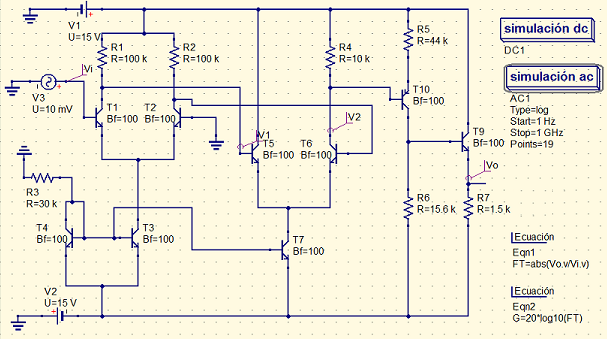
Finally, the output graphs corresponding to the frequency response of the output signal as a function of the input signal (FT) and the same value but in decibels (G) are observed.
Thank you for your attention, I hope this material will be useful and we will see you in a next tutorial.
Annexed the Nextlist PSPICE code of the op amp amplifier circuit.
<_BJT T4 1 110 400 -49 -26 1 2 "npn" 0 "1e-16" 0 "1" 0 "1" 0 "0" 0 "0" 0 "0" 0 "0" 0 "0" 0 "1.5" 0 "0" 0 "2" 0 "100" 1 "1" 0 "0" 0 "0" 0 "0" 0 "0" 0 "0" 0 "0" 0 "0.75" 0 "0.33" 0 "0" 0 "0.75" 0 "0.33" 0 "1.0" 0 "0" 0 "0.75" 0 "0" 0 "0.5" 0 "0.0" 0 "0.0" 0 "0.0" 0 "0.0" 0 "0.0" 0 "26.85" 0 "0.0" 0 "1.0" 0 "1.0" 0 "0.0" 0 "1.0" 0 "1.0" 0 "0.0" 0 "0.0" 0 "3.0" 0 "1.11" 0 "26.85" 0 "1.0" 0>
<_BJT T3 1 230 400 8 -26 0 0 "npn" 0 "1e-16" 0 "1" 0 "1" 0 "0" 0 "0" 0 "0" 0 "0" 0 "0" 0 "1.5" 0 "0" 0 "2" 0 "100" 1 "1" 0 "0" 0 "0" 0 "0" 0 "0" 0 "0" 0 "0" 0 "0.75" 0 "0.33" 0 "0" 0 "0.75" 0 "0.33" 0 "1.0" 0 "0" 0 "0.75" 0 "0" 0 "0.5" 0 "0.0" 0 "0.0" 0 "0.0" 0 "0.0" 0 "0.0" 0 "26.85" 0 "0.0" 0 "1.0" 0 "1.0" 0 "0.0" 0 "1.0" 0 "1.0" 0 "0.0" 0 "0.0" 0 "3.0" 0 "1.11" 0 "26.85" 0 "1.0" 0>
<GND * 1 40 270 0 0 0 2>
<GND * 1 50 20 0 0 0 0>
<GND * 1 30 530 0 0 0 0>
<GND * 1 20 140 0 0 0 0>
<Vdc V1 1 140 20 -26 18 0 0 "15 V" 1>
<Vdc V2 1 100 530 -26 -50 0 2 "15 V" 1>
<_BJT T1 1 170 200 8 -26 0 0 "npn" 0 "1e-16" 0 "1" 0 "1" 0 "0" 0 "0" 0 "0" 0 "0" 0 "0" 0 "1.5" 0 "0" 0 "2" 0 "100" 1 "1" 0 "0" 0 "0" 0 "0" 0 "0" 0 "0" 0 "0" 0 "0.75" 0 "0.33" 0 "0" 0 "0.75" 0 "0.33" 0 "1.0" 0 "0" 0 "0.75" 0 "0" 0 "0.5" 0 "0.0" 0 "0.0" 0 "0.0" 0 "0.0" 0 "0.0" 0 "26.85" 0 "0.0" 0 "1.0" 0 "1.0" 0 "0.0" 0 "1.0" 0 "1.0" 0 "0.0" 0 "0.0" 0 "3.0" 0 "1.11" 0 "26.85" 0 "1.0" 0>
<_BJT T2 1 290 200 -49 -26 1 2 "npn" 0 "1e-16" 0 "1" 0 "1" 0 "0" 0 "0" 0 "0" 0 "0" 0 "0" 0 "1.5" 0 "0" 0 "2" 0 "100" 1 "1" 0 "0" 0 "0" 0 "0" 0 "0" 0 "0" 0 "0" 0 "0.75" 0 "0.33" 0 "0" 0 "0.75" 0 "0.33" 0 "1.0" 0 "0" 0 "0.75" 0 "0" 0 "0.5" 0 "0.0" 0 "0.0" 0 "0.0" 0 "0.0" 0 "0.0" 0 "26.85" 0 "0.0" 0 "1.0" 0 "1.0" 0 "0.0" 0 "1.0" 0 "1.0" 0 "0.0" 0 "0.0" 0 "3.0" 0 "1.11" 0 "26.85" 0 "1.0" 0>
<R R2 1 290 100 15 -26 0 1 "100 k" 1 "26.85" 0 "0.0" 0 "0.0" 0 "26.85" 0 "US" 0>
<R R1 1 170 100 15 -26 0 1 "100 k" 1 "26.85" 0 "0.0" 0 "0.0" 0 "26.85" 0 "US" 0>
<_BJT T5 1 430 260 8 -26 0 0 "npn" 0 "1e-16" 0 "1" 0 "1" 0 "0" 0 "0" 0 "0" 0 "0" 0 "0" 0 "1.5" 0 "0" 0 "2" 0 "100" 1 "1" 0 "0" 0 "0" 0 "0" 0 "0" 0 "0" 0 "0" 0 "0.75" 0 "0.33" 0 "0" 0 "0.75" 0 "0.33" 0 "1.0" 0 "0" 0 "0.75" 0 "0" 0 "0.5" 0 "0.0" 0 "0.0" 0 "0.0" 0 "0.0" 0 "0.0" 0 "26.85" 0 "0.0" 0 "1.0" 0 "1.0" 0 "0.0" 0 "1.0" 0 "1.0" 0 "0.0" 0 "0.0" 0 "3.0" 0 "1.11" 0 "26.85" 0 "1.0" 0>
<_BJT T6 1 550 260 -49 -26 1 2 "npn" 0 "1e-16" 0 "1" 0 "1" 0 "0" 0 "0" 0 "0" 0 "0" 0 "0" 0 "1.5" 0 "0" 0 "2" 0 "100" 1 "1" 0 "0" 0 "0" 0 "0" 0 "0" 0 "0" 0 "0" 0 "0.75" 0 "0.33" 0 "0" 0 "0.75" 0 "0.33" 0 "1.0" 0 "0" 0 "0.75" 0 "0" 0 "0.5" 0 "0.0" 0 "0.0" 0 "0.0" 0 "0.0" 0 "0.0" 0 "26.85" 0 "0.0" 0 "1.0" 0 "1.0" 0 "0.0" 0 "1.0" 0 "1.0" 0 "0.0" 0 "0.0" 0 "3.0" 0 "1.11" 0 "26.85" 0 "1.0" 0>
<_BJT T7 1 480 420 8 -26 0 0 "npn" 0 "1e-16" 0 "1" 0 "1" 0 "0" 0 "0" 0 "0" 0 "0" 0 "0" 0 "1.5" 0 "0" 0 "2" 0 "100" 1 "1" 0 "0" 0 "0" 0 "0" 0 "0" 0 "0" 0 "0" 0 "0.75" 0 "0.33" 0 "0" 0 "0.75" 0 "0.33" 0 "1.0" 0 "0" 0 "0.75" 0 "0" 0 "0.5" 0 "0.0" 0 "0.0" 0 "0.0" 0 "0.0" 0 "0.0" 0 "26.85" 0 "0.0" 0 "1.0" 0 "1.0" 0 "0.0" 0 "1.0" 0 "1.0" 0 "0.0" 0 "0.0" 0 "3.0" 0 "1.11" 0 "26.85" 0 "1.0" 0>
<R R4 1 550 100 15 -26 0 1 "10 k" 1 "26.85" 0 "0.0" 0 "0.0" 0 "26.85" 0 "US" 0>
<_BJT T9 1 780 240 8 -26 0 0 "npn" 0 "1e-16" 0 "1" 0 "1" 0 "0" 0 "0" 0 "0" 0 "0" 0 "0" 0 "1.5" 0 "0" 0 "2" 0 "100" 1 "1" 0 "0" 0 "0" 0 "0" 0 "0" 0 "0" 0 "0" 0 "0.75" 0 "0.33" 0 "0" 0 "0.75" 0 "0.33" 0 "1.0" 0 "0" 0 "0.75" 0 "0" 0 "0.5" 0 "0.0" 0 "0.0" 0 "0.0" 0 "0.0" 0 "0.0" 0 "26.85" 0 "0.0" 0 "1.0" 0 "1.0" 0 "0.0" 0 "1.0" 0 "1.0" 0 "0.0" 0 "0.0" 0 "3.0" 0 "1.11" 0 "26.85" 0 "1.0" 0>
<_BJT T10 1 680 170 8 -26 1 0 "pnp" 0 "1e-16" 0 "1" 0 "1" 0 "0" 0 "0" 0 "0" 0 "0" 0 "0" 0 "1.5" 0 "0" 0 "2" 0 "100" 1 "1" 0 "0" 0 "0" 0 "0" 0 "0" 0 "0" 0 "0" 0 "0.75" 0 "0.33" 0 "0" 0 "0.75" 0 "0.33" 0 "1.0" 0 "0" 0 "0.75" 0 "0" 0 "0.5" 0 "0.0" 0 "0.0" 0 "0.0" 0 "0.0" 0 "0.0" 0 "26.85" 0 "0.0" 0 "1.0" 0 "1.0" 0 "0.0" 0 "1.0" 0 "1.0" 0 "0.0" 0 "0.0" 0 "3.0" 0 "1.11" 0 "26.85" 0 "1.0" 0>
<R R6 1 680 350 15 -26 0 1 "15.6 k" 1 "26.85" 0 "0.0" 0 "0.0" 0 "26.85" 0 "US" 0>
<GND * 1 360 230 0 0 0 0>
<.DC DC1 1 840 40 0 39 0 0 "26.85" 0 "0.001" 0 "1 pA" 0 "1 uV" 0 "no" 0 "150" 0 "no" 0 "none" 0 "CroutLU" 0>
<Vac V3 1 80 140 -26 18 0 0 "10 mV" 1 "1000 Hz" 0 "0" 0 "0" 0>
<R R3 1 70 300 -26 15 0 0 "30 k" 1 "26.85" 0 "0.0" 0 "0.0" 0 "26.85" 0 "US" 0>
<R R7 1 780 350 15 -26 0 1 "1.5 k" 1 "26.85" 0 "0.0" 0 "0.0" 0 "26.85" 0 "US" 0>
<R R5 1 680 70 15 -26 0 1 "44 k" 1 "26.85" 0 "0.0" 0 "0.0" 0 "26.85" 0 "US" 0>
<Eqn Eqn1 1 880 400 -26 15 0 0 "FT=abs(Vo.v/Vi.v)" 1 "yes" 0>
<Eqn Eqn2 1 880 490 -26 15 0 0 "G=20*log10(FT)" 1 "yes" 0>
<GND * 1 930 320 0 0 0 0>
<.AC AC1 1 850 120 0 39 0 0 "log" 1 "1 Hz" 1 "1 GHz" 1 "19" 1 "no" 0>
<R R8 1 890 310 -26 15 0 0 "50 Ohm" 1 "26.85" 0 "0.0" 0 "0.0" 0 "26.85" 0 "US" 0>
</Components>
<Wires>
<140 340 140 400 "" 0 0 0 "">
<110 340 120 340 "" 0 0 0 "">
<110 340 110 370 "" 0 0 0 "">
<110 430 110 480 "" 0 0 0 "">
<110 480 170 480 "" 0 0 0 "">
<230 430 230 480 "" 0 0 0 "">
<140 400 190 400 "" 0 0 0 "">
<120 340 140 340 "" 0 0 0 "">
<120 300 120 340 "" 0 0 0 "">
<100 300 120 300 "" 0 0 0 "">
<40 270 40 300 "" 0 0 0 "">
<230 270 230 370 "" 0 0 0 "">
<170 20 240 20 "" 0 0 0 "">
<240 20 240 60 "" 0 0 0 "">
<130 530 170 530 "" 0 0 0 "">
<170 480 230 480 "" 0 0 0 "">
<170 480 170 530 "" 0 0 0 "">
<50 20 110 20 "" 0 0 0 "">
<30 530 70 530 "" 0 0 0 "">
<20 140 50 140 "" 0 0 0 "">
<170 270 230 270 "" 0 0 0 "">
<170 230 170 270 "" 0 0 0 "">
<110 140 140 140 "" 0 0 0 "">
<140 140 140 200 "" 0 0 0 "">
<230 270 290 270 "" 0 0 0 "">
<290 230 290 270 "" 0 0 0 "">
<320 200 360 200 "" 0 0 0 "">
<240 60 290 60 "" 0 0 0 "">
<290 60 290 70 "" 0 0 0 "">
<290 130 290 170 "" 0 0 0 "">
<170 60 240 60 "" 0 0 0 "">
<170 60 170 70 "" 0 0 0 "">
<170 130 170 150 "" 0 0 0 "">
<170 150 170 170 "" 0 0 0 "">
<190 350 320 350 "" 0 0 0 "">
<190 400 200 400 "" 0 0 0 "">
<190 350 190 400 "" 0 0 0 "">
<170 150 400 150 "" 0 0 0 "">
<240 20 430 20 "" 0 0 0 "">
<400 200 400 260 "V1" 430 220 48 "">
<320 350 320 420 "" 0 0 0 "">
<320 420 450 420 "" 0 0 0 "">
<550 290 550 350 "" 0 0 0 "">
<480 350 550 350 "" 0 0 0 "">
<480 350 480 390 "" 0 0 0 "">
<550 130 550 150 "" 0 0 0 "">
<550 20 550 70 "" 0 0 0 "">
<430 350 480 350 "" 0 0 0 "">
<430 290 430 350 "" 0 0 0 "">
<170 530 480 530 "" 0 0 0 "">
<480 450 480 530 "" 0 0 0 "">
<680 20 680 40 "" 0 0 0 "">
<550 20 680 20 "" 0 0 0 "">
<680 100 680 140 "" 0 0 0 "">
<650 150 650 170 "" 0 0 0 "">
<550 150 550 230 "V2" 580 190 71 "">
<550 150 650 150 "" 0 0 0 "">
<680 240 750 240 "" 0 0 0 "">
<680 200 680 240 "" 0 0 0 "">
<780 20 780 210 "" 0 0 0 "">
<680 20 780 20 "" 0 0 0 "">
<680 240 680 320 "" 0 0 0 "">
<780 270 780 310 "Vo" 810 270 30 "">
<680 380 680 530 "" 0 0 0 "">
<480 530 680 530 "" 0 0 0 "">
<780 380 780 530 "" 0 0 0 "">
<680 530 780 530 "" 0 0 0 "">
<360 200 360 230 "" 0 0 0 "">
<580 260 620 260 "" 0 0 0 "">
<620 180 620 260 "" 0 0 0 "">
<320 170 320 180 "" 0 0 0 "">
<290 170 320 170 "" 0 0 0 "">
<320 180 620 180 "" 0 0 0 "">
<400 150 400 200 "" 0 0 0 "">
<430 20 550 20 "" 0 0 0 "">
<430 20 430 230 "" 0 0 0 "">
<780 310 780 320 "" 0 0 0 "">
<930 310 930 320 "" 0 0 0 "">
<920 310 930 310 "" 0 0 0 "">
<780 310 860 310 "" 0 0 0 "">
<110 140 110 140 "Vi" 140 110 0 "">
</Wires>
<Diagrams>
</Diagrams>
<Paintings>
</Paintings>
Curriculum
- Qucs simulator for semiconductor electronic circuits: Introduction
- Stages of design of a source regulated with Zener, using QUCS.
- Design of an amplifier of audio with Qucs
Posted on Utopian.io - Rewarding Open Source Contributors
Your contribution cannot be approved because it does not follow the Utopian Rules.
You can contact us on Discord.
[utopian-moderator]