History of Nvidia... The World's BEST Graphics Manufacturer! - History of Tech - Part 10
Nvidia is the worlds largest and most respected Graphics card manufacture in the world to date. If it wasn't for this company, many of the games you play may not of existed as the majority of them are made and rendered with an Nvidia GPU.

So lets look at Nvidia through the ages from the year before I got my first Nvidia GPU expansion card back in 2000.
1999 - GeForce 256.
The 256 was released in October of 99. it was hailed as the worlds first 'Graphics Processing Unit' (GPU) that was independent of the CPU.
The 256 name is derived from the 256 bit rendering engine that used 4, 64 bit pixel pipelines. This meant that the card was capable of rendering over 10 million polygons on screen per second with complete cube environment mapping. Today that may not sound like a lot, but in 1999, this was a huge leap forward in PC technology.
When compared to other 3D accelerators of the time, such as the 3DFx Voodoo3 3500 and the Riva TNT2 Ultra, the 256 boosted frame rate by up to 50%, some times more in titles that took advantage of the new 256 hardware.
The card featured 220nm construction, 4x AGP PCI, 120Mhz core clock and 166 memory clock, with a memory size of 64Mb and a bus width of 128bit,
This was the start of things to come from Nvidia and it only just got better from here on in.

Image Source
2000 – GeForce 2 Ti.
The following year the flagship 256 was replaced with the GeForce 2 Ti. It used a similar architecture to the 256, but with some notable improvements. The pixel piplines now had 2 texture mapping units each, making a total of 8. This meant the card was able to double up on the amount of textures seen on screen.
The card featured a 180nm construction, 4x AGP PCI, 250Mhz core clock with 230 Memory clock, 64Mb of memory, 128 bit bus speed and all this adds up to a 40% increase in performance over the 256.

Image Source
2001 – GeForce 3 Ti 500
The 3rd generation of the GeForce saw an advancement in the architecture from gen 2, this time, programmable pixel and vertex shaders, multi sampling, anti aliasing, which improved the cards performance even further. It was also the first card to offer full compatibility with Microsoft's Direct 3D 8.0. this enabled devs to create unique visual effects using Microsoft's shader 1.1. to enable the backwards compatibility to Direct3D 7, all the necessary hardware from gen 2 was included.
It featured a new 150nm construction which enabled it to bump up the transistor count to 57 million, AGP 4x PCI interface, 240Mhz core clock with a Memory clock of 250Mhz, the memory size had been doubled to 120Mb with the same 128 bit bus.

Image Source
2002 – GeForce 4 Ti 4200 8X.
This was the year that Nvidia expanded there product range that included both low end and enthusiast grade cards to choose from. The forth gen GeForce card was similar to the gen 3, but with much higher core and memory clocks, better support from Direct 3d 8.0, much better memory controller and an overhaul on the rest of the support shaders, anti aliasing, legacy support and more.
It had the same 150nm construction, but it had a core clock of 250Mhz and memory clock of 250Mhz also, this time with an AGP 8x PCI interface, 128MB memory, and with a 128bit bus. With all the improvements made, the card was on average 20% faster and more capable than the gen3.

Image Source
2003 – GeForce FX 5950 Ultra.
2003 saw the introduction of the FX series from Nvidia. This is the 5th generation to hold the GeForce title, but it was the first GPU that was fully compatible with the new Microsoft Direct3D 9.0, better known as Direct X 9.
This was also the first card that would be compatible with DDR2, GDDR3 and GDDR5. The FX range saw the first dual slot GPU expansion card to accommodate a larger cooling heat sink and fan.
A new 130nm construction was implemented in this card, seeing a rise in the number of transistors at a whopping 135 million that made up the Rankine architecture. The core clock was set to 475Mhz and so did the memory clock. An AGP x8 interface, 256Mb of memory and the Bus speed had been doubled to 256bit. This all added up to a performance increase of nearly double that of the previous gen.

Image Source
2004 – GeForce 6800 Ultra.
As time moves on, so does the manufacturing process for Nvidia's GPU's. The 6th Gen GPU line up, the 6000 series as its better known, introduced the Scalable Interface Link or SLI, which enabled users to use 2 GPU's to improve overall performance when used with the PCI Express interface bus.
Other new technology included PureVideo to decode various encoders like H.246, WMV, MPEG-2 among others, and shader Model 3.0 which worked with both Direct X 9.0c and Open GL 2.0.
The transistor count had grown to 222 million while still using the same 130nm construction. The interface bus had improved over to the PCI Express bus with x16 PCI lanes. The core clock had dropped slightly to 400Mhz to cope with the increased heat. The memory had a core clock of 525Mhz with 512Mb of new GDDR3 Memory all going through a 256bit bus.

Image Source
2005 – GeForce 7800 GTX.
This was about the time in GPU development when people were starting to say... 'HOLY CRAP!'. The 7000 series and 7th Gen GPU was the last line up that used the now out dated AGP bus interface. As well as the improved SLI technology, they had also added Intellisample which is the first type of super sampling, (also used on the 6000 series cards that were released in 2005) and Turbo Cache which allowed the GPU to utilize both GPU memory and system memory to help with Buffering but only on the cards that used the PCIe Bus Interface.
Transistor count now stood at a tad over 300 million using the all new 110nm construction. Core clock stood at 550Mhz with the memory getting a huge boost to 850Mhz with 512Mb of GDDR3 through a 256bit bus. Not a great performance increase at only 15-20%, but the capabilities of the card were very impressive.

Image Source
2006 – GeForce 8800 GTX.
Released very late on in the year, the 8000 series, 8th gen flagship GPU hit the market with an all new Tesla Architecture that improved performance tenfold... well. Increased by a good margin over the last gen.
The new display capabilities support 10bit for each channel output, a step up from the 8-bit of the previous gen. This allowed a much crisper and higher fidelity on compatible and multiple displays. The PureVideo had also been improved to help with decoding HD videos of 780p/1080p or higher.
The construction size of the transistors had been decreased even further to 90nm but had over 680 million transistors on a huge 484mm2 die. At the time, this was the largest GPU chip ever constructed. It was almost the width of the cards PCB. The core count had increased to 612Mhz while the memory received another huge boost up to 1080Mhz with 768Mb of GDDR3 memory all through a new bus of 384bit. This was all a huge leap in performance of over 90% compared to the previous flagship and would stay with us for another 2 years, some are even still in use today. That's how good it was.
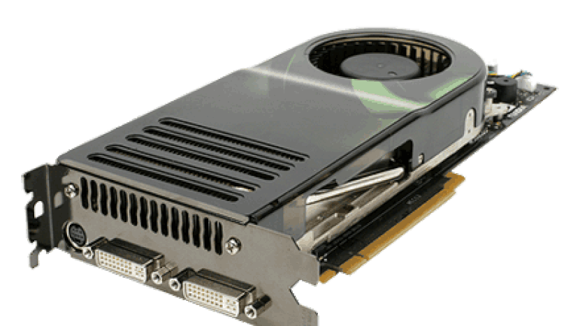
Image Source
2008 – GeForce 9800 GTX.
With such huge success and popularity with there previous gen card, they took there time before releasing there next flagship, 2 years later. This was the generation that saw the introduction of Cuda Cores that are responsible for processing all the data in and out of the GPU. Similar to a CPU with 8, 10, 12 or more cores but many more. The Tesla architecture is still there, only slightly improved as it was already good to begin with.
It is built on a 65nm construction (55nm in 2009) with a transistor count of 754 million, so not a huge increase. The interface bus now supports PCIe 2.0. core clock of 738Mhz and memory clock of 1100Mhz with a full Gb of GDDR3 memory through a slimmed down 256bit bus as the card is more streamlined and efficient over the last one. It also supports Direct X 10 and Open GL3.3. Only a slight improvement in performance, but why fix what isn't broken.

Image Source
2009 – GeForce GTX 295.
Skipping over the 100 series as it was just a rebrand of the same 9000 series card, the 200 series, and Nvidia's 2nd generation Tesla based architecture, but the first to receive a Unified Shader Architecture that handles all the shading processes increasing performance, the biggest update since the 8000 series.
This one kept the 55nm construction as seen on the later 9000 series, but with 2, yes 2 GPU chips on a single PCB. Each die has 1.4 Billion transistors, and each die is an impressive 470mm2 in size. Core clock stands at 576Mhz and memory is at 1998Mhz with 2Gb of GDDR3 that is all pushed through 2x 448bit buses. An impressive card that blew everything out of the water with its awesome power at the time.

Image Source
2010 – GeForce GTX 480.
Skipping over the 300 series as it was a 200 series rebrand, the new 400 series cards came out early 2010 with an all new architecture called ''Fermi''. It included very large number of stream processors, 512 to be exact, in groups of 32. Nvidia dubbed this card ''as the next big leap in graphics card design''. The card had all new ECC (Error correcting code) to either fix or dump any errors found in the memory, and had support for Visual Studio and Microsoft's C++ programming language, making it easier for game devs to create infrastructure code within the games programming.
Transistors had a big jump up to 3 billion on a massive 529mm2 die with a 40nm construction. The core has a 700Mhz Clock Speed, and a memory clock of 3.4Ghz with 1.5Gb of all new and much faster GDDR5 memory through a 384bit bus. It also included a much larger heat sink that coverd the whole PCB.

Image Source
2011 – GeForce GTX 590.
the 500 series is a natural progression over the 400 series and the Fermi architecture, but heavily modified. The 500 series could all now support Dirext X 12, OpenGL 4.6 and OpenCL 1.1.
Unlike the 580 which was released late 2010. the 590 featured another dual GPU chip design with an much improved bridge allowing data to flow much faster without restriction.
As well as having doubled up on the GPU chips, each chip had 3 Billion transistors with the same 40nm construction process on a slightly smaller 520mm2 die. Each core was clocked to 607Mhz, while the 3GB of GDDR5 memory (split between the 2 GPU's) ran at 3.4Ghz all running through 2 384bit buses. This all meant that the card had a 30 – 40% increase in performance over the 480 and 580.

Image Source
2012 – GeForce GTX 690.
A new year, a new flagship card, a new series and all new architecture which was called Kepler, named after the scientist and the space telescope. Fermi was designed with raw power and performance in mind, Kepler took it a step further by increasing the performance per watt. This was achieved by getting rid of the shader clock found on previous cards, and having a unified clock instead. According to Nvidia, 2 Kepler GPU's use 90% of the power as one Fermi GPU. This massive reduction in power is thanks to the reduced clock speed, but now they have to increase the core count to achieve better performance over the Fermi architecture.
Every card in the 600 series added features such as PCIe 3.0 interface, HDMI for 4k streaming, Display port 1.2, Support for up to 4 Monitors/displays, TXAA in game abilities, and much more.
The new 28nm construction was the key ingredient in the Kepler design. The twin GPU's had 3.54 billion transistors on a much smaller 294mm2 die when compared to Fermi. The core is clocked at 915Mhz with the ability to boost up to 1058Mhz. The 4Gb of GDDR5 memory is clocked at 1.5Ghz threw 2x 256bit buses. This new design while lower on power consumption was only on average 10% better performance over the 590 from the previous year.

Image Source
2013 – GeForce GTX Titan.
The 700 series ran on a much improved and polished Kepler design architecture that improved all the aspects of the 1st gen Kepler architecture. There is now an increase in memory size and a wider bandwidth to allow much higher computational performance while keeping the power consumption low that made the 600 series so good.
As well as having all the same features as the 600 series, there has also been a few more added and improved, such as Cuda compute 3.5 capabilities, Hyper Q that improved CPU connectivity, GPUDirect from Nvidia, SMX improvement and Dynamic Parallelism.
While still working with the 28nm construction, the core transistor count had risen to over 7 billion on the biggest die to date at 561mm2 and had a core clock of 837Mhz boosted up to 993Mhz. The 6Gb of GDDR5 memory ran at a clock of 1.5Ghz through a 384bit bus. The TitanZ which was released the following year had dual GPU designed was immensely powerful and could take a 1080 from today and give it a run for its money.

Image Source
2015 – GeForce GTX 980 Ti.
The 700 series stayed with us for 2 years, and Nvidia made the decision to skip the 800 series (which was mobile only) and go straight into the 900 with a slimmed down selection of cards. The New Maxwell design architecture was a massive improvement over the 600 and 700 series cards with improved power efficiency, better graphical capabilities and easier programming. While the first GPUs using the Maxwell architecture were released in 2014, it wasn't until 2015 when they released the new flagship card, the 980 ti, and the Titan X which was ridiculously expensive.
The biggest improvement was in the native shared memory for both 32 and 64bit compare and swap (CAS) which utilises the system memory and the GPU memory more efficiently, meaning more performance along the 32 memory lanes at 28Gb/s.
Again it had a 28nm construction process, but with 8 billion transistors on the largest Die on any GPU at 601mm2. The core clocked at 1Ghz, with a 1.2Ghz boost. The 6Gb of GDDR5 memory is clocked at 1.75Ghz and has a bus width of 384bit. The power consumption is less than its predecessors, but the overall performance was on average 12 – 15% better. So good in fact, that many people are still using this particular card and don't want to upgrade until the next gen GPU comes out in 2018.

Image Source
2016 – GeForce 1080 Ti.
The current top end card and current king in the graphics world is the renowned 1080 Ti using quite possibly the best design architecture to date, Pascal. So good in fact that we have to wait 3 years before it is replaced or renewed for the next gen GPU.
The 1080 features Cuda Compute 6.0 and 6.1, display port 1.4, HDMI 2.0b which is capable of streaming 8k. (Though I could be wrong). HDCP support for 4K DRM, NVEC 10bit hardware encoding, great for video editors. HB SLI bridge. GDDR5 and GDDR5X memory support.
Triple Buffering system that can also work with Vsync. And a whole host of other features.
The smallest construction process to date of 16nm is found on this card (but the new 1030, 1050 have even smaller 14nm) and 12 billion transistors on a 471mm2 die. The core is clocked at an impressive 1.48Ghz that can be boosted up to 1.65Ghz. The 11GB of all new GDDR5X memory is clocked at 1.38Ghz through a 352bit bus.
The 1080 Ti is a very sort after GPU in today's market as many PC gamers want a fully immersive experience at the best possible detail, which the 1080 Ti can deliver with ease.

Image Source
Nvidia's history is full of enhancement, improvement and the ability to create something that is truly astounding to the point, every PC gamer, programmer, editor and more want a slice of it.
Thanks for reading.

Stu @TechMojo
Join the chat TechMojo Discord Channel
Follow us TechMojo OnG Social Page
Like us TechMojo Facebook Page
Follow us TechMojo Twitter
I remember my good old Voodoo 😊
nice