SEMICONDUCTOR DEVICES
ENERGY BANDS IN SOLIDS
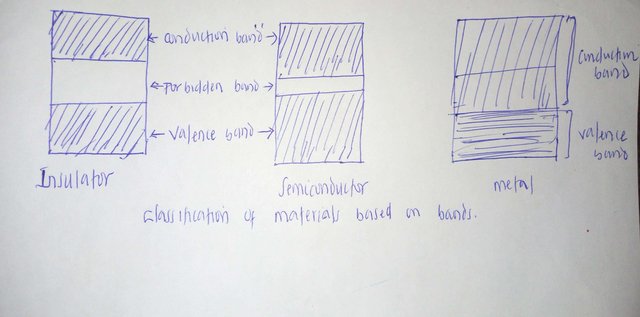
Many separate atoms are combined to form a solid. Between these overlapped atoms, there has to be series of interactions in such away that individual levels of energy of each atom extends to an energy bands comprising the Upper band (conduction band) and Lower band (valence band).The two bands may be separated by an energy gap called forbidden band gap which cannot be occupied by electrons.
Electrical materials are usually classified as Conductor, Semiconductor or Insulator according to their intrinsic ability to conduct electricity at room temperature. The class into which a material belongs depends on the behaviours of the valence electrons i.e. the electrons in the outermost orbit of the atoms.
In an insulator, the valence electrons are tightly bound to the nucleus and thus the valence band is completely filled with electrons while the conduction band is empty. The two bands are separated by a wide gap. The electrons in the valence band have thermal energy of the order KT where K is the Boltzmann and T is temperature in Kelvin. At room temperature, the forbidden band is much greater than KT in magnitude hence electrons in the valence band are unable to gain sufficient energy from the applied voltage to move into the conduction band. Consequently, insulators are unable to conduct at room temperature.
Semiconductors are a group of materials having electrical conductivities intermediate between metals and insulators . The conductivity of these materials can be varied over orders of magnitudes by changes in temperature , optical excitation and impurity content. Semiconductor materials have a narrow forbidden gap between the valence and the conduction bands, the enegy gap is of order KT.
At 0K, all electrons are in the valence band and the material is then an insulator. At room temperature, however, some of the valence electrons are able to acquire sufficient thermal energy which they use to move into the conduction band where they become free electrons. In place of liberated electrons, holes are created in the valence band . The conduction of electricity in semiconductor is due to movement of free electrons and holes.

Source: @thestronics
Metals are excellent conductor of electricity. In metals , the conduction and valence bands overlap such that at all temperature above absolute zero, electrons are always readily available in the conduction band. Also, the valence electrons are weakly bound to the parent atoms in metals such that a slight potential difference across a conductor causes the free electrons to constitute electric current.

Source: @thestronics
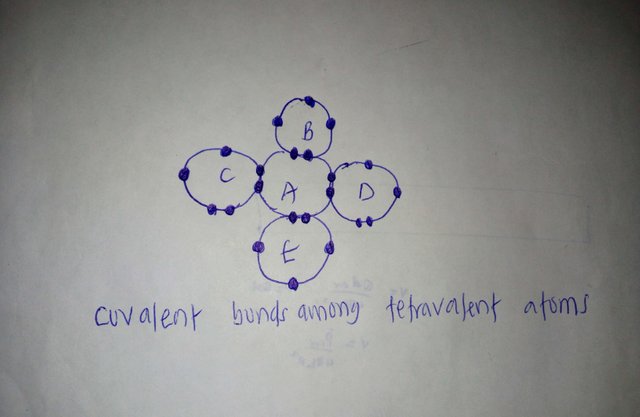
Atoms of intrinsic semiconductor materials are tetravalent. As shown above, a tetravalent atom A share its four valence electronswith atoms B,C,D and E in order to attain stable outer octet of eight electrons. Although, each atom has four valence electrons, after bonding, each atom will have four electron-pairs surrounding it. Each electron-pair is referred to as a covalent bond. These covalent bonds keep the atoms together in crystal formation.
CONDUCTION IN INTRINSIC SEMICONDUCTOR MATERIAL
In an intrinsic or pure semiconductor at 0K, all the valence electrons are tightly bound to their parent atoms and the semiconductor behaves an an insulator. As the temperature is increased, some of the valence electrons are able to break their covalent bonds and move from the valence band into the conduction band where they become free electrons .
An electron moving from the valence band into the conduction band leaves a free hole in the valence band. A free charge (electron or hole) is one that is not tightly bound to any atom and is able to move freely through the material. Further increase in the temperature causes more electrons to break away their atoms and become free electrons which results into generation of more electron-hole pairs. The thermally generated charges move randomly in the semiconductor.
In an intrinsic semiconductors, n==p==ni
Where n= concentration of electrons
P= concentration of electrons
ni= intrinsic carrier concentrations
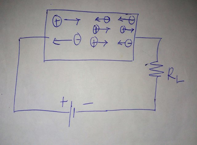
If a battery Is connected across the ends of the semiconductor, an electric field is set up . The applied electric field draws the free electrons towards the positive terminal of the holes and are accelerated in opposite directions by the field, the resulting current flows in the same direction as shown below:

Source: @thestronics
CONDUCTION IN AN EXTRINSIC SEMICONDUCTOR
The number of free holes and electrons that are thermally generated in intrinsic or pure semiconductor crystals is very small at room temperature. The number of charge carriers can be considerably increased by purposely introducing impurities called dopants into the pure semiconductor crystals. The process is called doping. By dopping, a crystal can be altered such that it has predominance of either electrons or holes. And this leads to semiconductors types which is either p-type or n-type semiconductors.
THANKS FOR TAKING YOUR TIME TO READ!!!
REFERENCES

