PHOTOLITHOGRAPHY: THE PROCESS OF BRINGING CHIPS TO LIFE
Processors are one of the costliest components of any computer yet it is produced from one of the commonest element in this world, Silicon (sea sand). Intel describes process as the "process of turning sand to circuits". The major component of a processor is the transistor. The first Intel processor, the Intel 4004 was integrated with 2300 transistors but that was back in 1970.
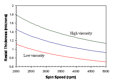
The Intel Core i7 Haswell-E Deca core processor has a transistor count of 3.2 billion while the AMD Epyc 32-core processor has a whooping transistor count of 19.2 billion! There's more; Intel's co founder, Gordon Moore in 1965 watched the trend of transistor integration and made a postulate that transistor count would double for every year and trend continued as he predicted. This was later termed the Moore's law (pictured right).))
I know you would be asking why transistors? Why in these quantities? How is it possible to incorporate billions of transistors in a device far smaller than a coin (yes, a coin. Qualcomm Snapdragon 835 mobile phone processor has more than 3 billion transistors). We use transistors because transistors are one of the fastest switching electronic device available and they can be made into very tiny microscopic shape. The computer is a digital machine, which means it can process data that are in discrete forms. Discrete in this term means a limited number (one and zero, off and on). Transistors can be made to process data and perform functions when they are switched on and off at a very high speed in a certain pattern.
Many transistors are incorporated into chips because transistors are not only used for switching. They also act as amplifiers. The transistors used in chips are in the form of logic gates. These gates are later grouped into logic blocks and these blocks are then grouped according to the functions they perform. These grouped functions are what is collectively called chips. So as the function of chip increases so do the number of transistors required to carry out these functions increases. And this explains why the 1970 Intel 4004 processor contained just 2300 transistors and the 2016 core i7 contained 3.2 billion transistors.
The process of making chips is called photolithography. Lets break it down a bit. Photolithography is a three Greek words combined into one which are photo, meaning light, litho meaning stone and graphy meaning writing. Combining these words, photolithography means the process of writing on stones using light.
The stone in this contest means sand built into stone-like structures called wafers. Wafers are 100% pure material formed from a crystalline material that are free from defects. To create defect-free and pure crystals, the crystals has to be grown in a process called the Czochralski process. After the growth, the resulting crystals is formed in the form of a cylindrical shape as shown in the image (right) and is later sliced into very thin shapes, mostly micron meters.))
The initial step in photolithography is the preparation of the substrate (wafer). The substrate are cleaned to remove any contamination using chemical compounds like the hydrogen peroxide. Dirts like the size of pin point will render the chips unusable. Chips are fabricated in a facility called fabs. Processors are manufactured in an ultra-clean facilities. In fact inside Intel's ultra clean fabs, the manufacturing processes are carried out in a cleanroom.
If the world map is printed in a paper as wide as a coin, a pin puncture of the paper could remove an area lager than a country! The same thing is applicable to chips since billions of components are compressed into a tiny structure, dirt is definitely a contamination. Engineers that works in fabs wear suits called bunny suits (pictured left). These suits were designed to keep hair and lints (tiny cloth strands) contamination away during the process. After the cleaning, the wafer is baked under temperatures between 200 and 400 degrees centigrade to remove water molecules and allowed to cool.))
The next procedure is the coating of the wafer with a photoresist. Photoresist are material that are sensitive to light. They are applied uniformly on the flat wafer using a process called spin coating.
This process involves rapidly spinning the wafer rapidly after the application of the photo resist. As shown in the image to the right, the speed of this spinning with respect to the resist viscosity is dependent on the desired thickness of the applied photoresist. When the desired thickness of the photoresist has been obtained, the wafer is transferred to another baking process where it is subjected to temperatures between 90 and 100 degrees centigrade and quickly cooled to remove excess photoresist.))
After the application of photoresist, the wafer is then subjected to an intense light in a desired patter. Before the application of the light, a mask with the desired pattern is aligned on the wafer. This masks creates patterns which later forms the desired component and connections for the chip.
This exposure process allows the film coated photoresist to be removed by a compound of diazonaphthoquinone which is a compound that reacts with light. This compound is called a "developer". The applied photoresist is usually of two types; the positive photoresist which is the most common type is usually soluble in the developer when exposed to light and the negative photoresist which desolves the unexposed portion of the wafer in the developer. The resulting structure is then subjected to a post exposure baking which helps remove tiny projections on the wafer caused by interference of incident light.))
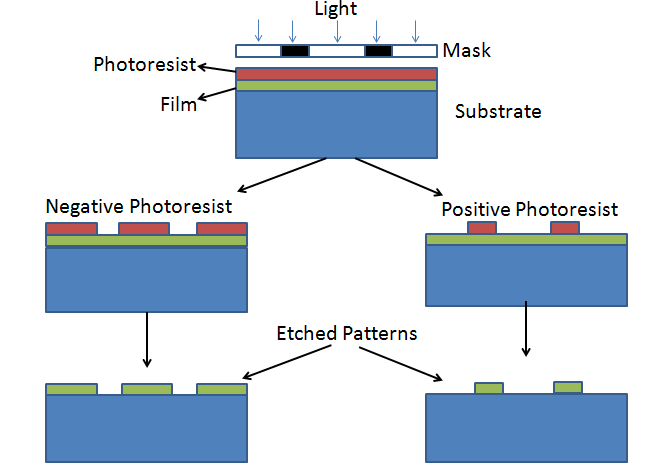
image credit:InTechOpen
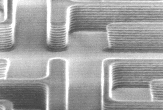
The final process involves etching and the removal of the remaining photoresist. Etching is the removal of the topmost layer of the substrate in the areas that are not covered by the photoresist as shown in the image above.
REFERENCES
- Photolithography - wikipedia
- lithobasics -Lithoguru
- Museum making silicon- Intel
- Logic gates -wikipedia

Good information.
thanks
I've Follow, Upvote. Interesting post. I like, multiply the article and expand it again. Spirit and keep working. Follow me @madimancity
thanks
great info...you shall throw more light when we see one on one...
On your last image you have
when it should be
<a href="source">thanks, correction taken
No problem! I have made mistakes like that in the past,