Procedure for the measurement of photoconductivity in semiconductor materials
Summary
Photoconductivity is a phenomenon in which a material becomes a better electrical conductor due to the absorption of electromagnetic radiation, it is defined as the change in the electrical conductivity (σ) of a material due to the incident radiation action, it occurs in semiconductors as a consequence of electron transitions induced by photons (of energy greater than the gap of the semiconductor) in which light is absorbed, additional charge carriers can be created (the electrons pass from the valence band to the conduction band). Measurement technique used in AC for very low signal materials, most of the existing materials. They consist of modulating the incident light and measuring the current to this modulation, this technique is widely used in high speed response materials.
Introduction
The conductivity of semiconductor materials depends on the number of conduction band electrons and also on the number of gaps in the valence band, the thermal energy associated with the network vibrations can excite the electrons and generate gaps and / or free electrons, as a consequence of electronic transitions induced by photons in which light is adsorbed, additional charge carriers can be generated, this increase in conductivity is called photoconductivity. In this way when a photoconductive material is illuminated, the conductivity increases.
Photoconductivity is defined as the change in the electrical conductivity (σ) of a material due to the action of the incident radiation. The first report on photoconductivity occurred in 1873 by W. Smith, who observes that the resistivity was diminished by the effect of the sun's radiation.
The photoconductivity measurements that are proposed to be made is by an experimental technique, where a radiation source in the required spectral range, the hand-chromator, an intensity modulator, a conductivity cell, instruments needed to measure the signal produced by the sample are required. , are mounted for an alternating current configuration, this method the radiation from an arc lamp of Xe 1kw, in which instrumental spectrometry is used as an excitation source, a SRS830DPS sw blocking, and an amplifier for signal measurement.
The photoconductivity is measured by the variation of the switching frequency of the incident light from 1 Hz onwards and it can be found that T reaches a maximum threshold value for a particular frequency (fmax) above or below which photocurrent occurs. The support life time (T) is given by:
T=1/2pi fmax
The basic principle on which photoconductivity is based is very simple:
When a photon of energy greater than or equal to the material gap impinges on a semiconductor it can be absorbed by the material, passing an electron to the conduction band, leaving a gap (void) in the valence band; these two carriers contribute to the increase in the conductivity of the material. In this case the conductivity is called intrinsic.
In the case of materials with defects, impurities or any type of distortion, it may happen that a photon of energy less than the material gap is absorbed and the electrons pass to the conduction band or gaps are formed in the valence band, in this case case only one type of carrier is increased. This process gives rise to extrinsic photoconductivity.
From the previous explanation it can be seen that the phenomenon of photoconductivity is a complicated process within the semiconductor since it originates from the balance between the generation of free carriers and their subsequent recombination.
Source
Experimental Methodology
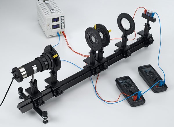
- Mount the circuit of the figure, be careful not to damage the surface of the material.

Source
Important: Take care that the radiation does not affect the contacts
- Check the ohm law in the contacts in the dark.
- Measure the residual conductivity (residual or dark current Io)
- Measure the steady state photoconductivity for each wavelength
- Measure the lamp signal for each wavelength, correct according to the detector response (using a rule of three)
- Calculate the corrected photoconductivity at a given lamp intensity, generally 1 mW / cm2, calculate the approximate material gap.
- For two wavelengths, measure the transient photoconductivity in both the rise and the decay, graph and calculate the recombination time.

Source
References:
W.D. Callister. “Introducción a la ciencia de los materiales 2”editorial REVERTE.
J.L.Solis “física de células fotovoltaicas” universidad nacional de ingeniería, instituto peruano de energía nuclear.
J. E. Rodríguez. "Los óxidos cerámicos como materiales termoeléctricos". Rev. Acad. Colomb. Cienc.: 31 (121), 545-555, 2007.
N. Auparay. "Room Temperature Seebeck Coefficient Measurement of Metals and Semiconductors". Tesis, pp. 26, 2013.
B. M. Amoli, S. Gumfekar, A. Hu, Y. N. Zhoubc and B. Zhao. "Thiocarboxylate functionalization of silver nanoparticles: effect of chain length on the electrical conductivity of nanoparticles and their polymer composites". J. Mater. Chem., 22, 20048-20056, 2012.
Measuring the Resistivity and Determining the Conductivity Type of Semiconductor Materials Using a Four-Point Collinear Probe and the Model 6221 DC and AC Current Source. Application Note Series, Keithley, Number 2615, 2005
muy buena información , siempre es un placer seguir tu contenido, saludos...
Que bueno que te gusto. Saludos
My little vote for you, my friend, a greeting and many successes @katiuskagomez
Thanks friend