FROM SAND TO THE SILICON WAFER
In this post, I present a brief discussion on the main aspects behind the solar technologies, before a solar cell is produced: silicon wafer manufacture. Due to the electronic and optical properties, silicon is the most employed material in whole electronic and photovoltaic industries. The production of a silicon wafer for solar cell applications is not a simple task, sinceseveral complex and expensive processes are involved: 1) extraction of silicon from sand; 2) purification of the raw silicon; 3) crystallization; 4) wafering. After a short journey through history and some applications of silicon, I briefly describe all four processes in the silicon wafer production.
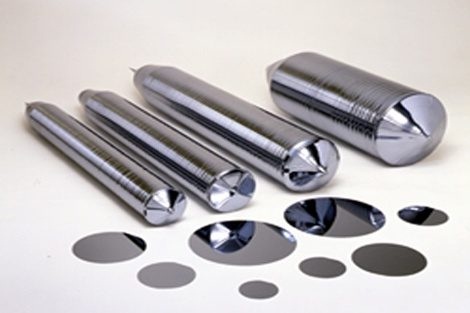
A breaf history
Since the discovery of photoconductivity in selenium (Se), by W. Smith in 1873, the possibility of using light to produce electric energy gained much attention in the whole scientific and engineering community. And few years later (1876), William Adams and Richard Day observed the first photovoltaic current in Se. But, it was until 1883 when the american scientist Charles Edward Fritts, invented a photovoltaic device that resemble what we have known later as a solar cell. Fritts´ invention consisted in a selenium film compressed between a brass plate and a gold film, such as in Figure 1.
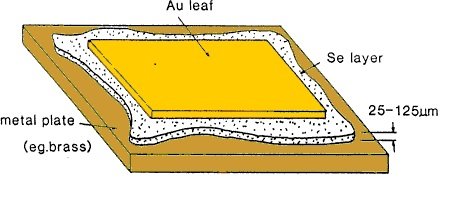
Figure 1.Charles Fritts´ photovoltaic cell (Figure credits: David Rosengrant, Walmart Foundation Sustainable Homes Project, Kennesaw State University, [email protected], 2010)
This experiment was easy to be implemented, and the electric current could be stored in batteries for later use. However, no more than 0.1% of light could be converted into electric energy. During incoming years, considerable theoretical and experimental work was performed in quantum physics and solid state physics, in order to find a new material with better photovoltaic properties. The fabrication of the first silicon solar cell was reported in 1941 by Ohl, et. al, when working on melt-grown p-n junctions, with conversion efficiency of the order of 1%. A decade later, Daryl Chapin, Calvin Fuller, and Gerald Pearson, from Bell Labs, created p-type and n-type silicon photovoltaic cell with efficiencies of about 4.5% and 6%, respectively [1], and then in 1960 engineers working at Hoffman Electronics enhanced this efficiency up to 11% in n-type silicon cells [2], few years later the first solar cell array Gunnar Michelson, also at Hoffman presented his first solar cell array [3]. These facts are considered by many historians as the beginning of the multimillionaire silicon-market. Nowadays, silicon has turned to be the most demanded material for PVC applications, and in the whole microelectronics industry.
Some properties and uses of silicon
Discovered by Jöns Jacob Berzelius in 1823, silicon is the most abundant element in Earth, following oxygen, with atomic number 14, and chemical symbol Si. This element is not properly a metal, but a semiconductor, with electrical properties between a metal and a dielectric. This particular feature has turned Si the most demanded material in the electronic industry. Si is naturally found as a compound called silica (SiO2), or quartz sand, so several physical and chemical processes are required to obtained poly (poly-Si) or crystalline silicon (c-Si) for industrial purposes. This silicon is then used in many applications such as [4-8]:
- the alloying of steel and cast iron,
- production of raw materials for PVC and microelectronic applications
- preparation of ceramics, cements, and glasses
- silicon carbide for abrasive materials
- Dental filling materials
From the chemical point of view, silicon shares chemical properties with carbon (C), giving to this element more specific applications, such as biomedical and therapeutic. Silicon is a vital component of living tissues, and it is found in the form of silica. It is fundamental in the constitution of the structure of our body: bones, muscles, nails, skin, connective tissues, etc. When consumed in the form of organic silica, it can be used in homeopathic therapies, repairing and cellular regeneration, and in the treatment of many diseases. Also, in some cases an artherosclerotic condition is usually related to the lack of silicon.
Obtaining silicon from sand
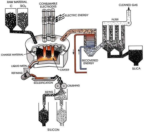
The primary processing step for the production of silicon from sand is the production of metallurgical-grade silicon via a metallurgical reductionprocess. The sand is first introduced in an electric-arc furnacewith carbon, at approximately 3000 C. As a consequence, the silicon is obtained according to the reaction

A deposit of liquid silicon is formed in the bottom of the furnace, and then extracted and cooled. The silicon produced in this process is metallurgical-grade silicon with a purity of 98-99% (100 ppm), and at a cost around 1-2 USD/Kg. Typical impurities in metallurgical-grade silicon include carbon, transition metals, boron and phosphorus [9]. Figure shows a typical industrial furnace for the production of metallurgical-silicon. A detailed description of this production process can be found in the literature [10]. This silicon is appropriate for the metallurgic industry in the production of special alloys, however, it is not useful for semiconductor and photovoltaic applications, since these requires high purities of the order of 0.001 ppm. This high purity silicon is obtained by means of several methods. However, two typical purifying processes are described here: a) Siemens process; b) Metallurgical process.
Figure 2.Industrial furnace used in the production of metallurgical-grade silicon (Figure credits: Ref. 9)
Siemens process is resumed in Figure 3. First, the metallurgical-grade silicon is milled into fine particles and then fluidized with hydrochloric acid (HCl) to produce trichlorosilane (SiHCl3), according to the reaction

Semiconductor-grade SiHCl3 in liquid state is then distilled in a series of distillation columns, before it is purified in a Siemens reactor at a temperature of 1150 C. In this step, the silicon is deposited in an inverted U-silicon rod, and purified following the inverse reaction,

What it is obtained from this process is polycrystalline electronic-grade silicon of purity 0.001 ppm or less.The Siemens method is a highly expensive method with prices of the order of 60-70 USD/Kg.
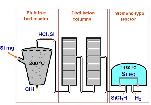
Figure 3.Simplified sketch of a Siemens process to produce electronic-grade silicon (Figure credits: Alba Ramos, PhD Thesis, 2016. DOI 10.13140/RG.2.1.3387.1122)
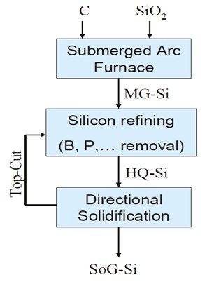
A less expensive method to obtain electronic-grade silicon from metallurgical-grade silicon, is the refining by metallurgical routes to remove the impurities (Fe, Al, Ti, Mn, B, P, O, and C) from the silicon matrix. The key technique of this process is the directional solidification [11] in a zone furnace. The process is temperature-controlled, and consists inmelting a silicon rod at 1500˚ C, moving slow down into the furnace. The liquid silicon is then cooled as this reaches the bottom of a quartz o graphite mold at 1000˚ C, while the impurities rise to the top of the mold. To first remove boron, phosphorus, oxygen, and carbon, the directional solidification process is preceded by acid bleaching and plasma refining [12]. After this purification, solidification process is then held in a graphite mold. High quality (HQ) silicon rich in metallic impurities is obtained. The second step consists in the removal of Fe, Al, Ti, and Mn, impurities from the HQ-silicon. For this, an ingot of HQ-silicon is processed in a second directional solidification. At this stage, other directional solidification processes can be combined to produce the desired purity. As a result, solar/electronic-grade silicon is obtained. It is expected that metallurgical routes became the dominant refining processes in the solar/electronic industry.
Figure 4. Metallurgical route to produce electronic/solar-grade silicon (Figure credits: Ref. 9)
Crystallization of silicon. The wafer
The high purity solar-grade silicon produced in the refining process described above, is polycrystalline and is not useful for photovoltaic applications. This is because solar cells need silicon wafers of good crystallographic quality, in order to achieve the higher efficiency. The production of crystalline silicon for the solar industry follows two basic steps:
Ingot crystallization. The crystalline quality of the silicon required in the solar industry can be both single-crystalline o multi-crystalline. Since single-crystalline silicon has superior quality, and with minimal structural defects compared to multi-crystalline silicon, we focus our attention in the production of single-crystalline silicon ingots. The most commonly used technique to grow single crystal from a polycrystal is the Czochralsky technique.Solar-grade silicon is melted inside a quartz crucible, at a controlled temperature just above the fusion temperature (1414 C). At this point, atoms of boron or phosphorus are added in order to obtain p-type or n-type silicon, respectively. A seed of single-crystalline silicon, fixed in the lower side of a vertical rod, is lowered into the liquid silicon. Once the seed is dipped into the surface of the molted silicon, is then slowly moved upwards and rotated in controlled motion. As this occursthe melt reach thermal equilibrium with the seed, and the material around the seed replays the seed´s crystalline structure. Finally, due to gravitya cylindrical single-crystalline ingot is obtained.All process is performed at an inert argon atmosphere, inside a quartz chamber.
Wafering. Once the single-crystalline solar-grade ingot has been prepared, the next step is wafer manufacturing. Basically, wafer manufacturing undergoes the following process. The cylindrical ingots are sliced in a multi-wire saw, with steel wires of 100-120 microns of diameter recovered with diamond particles of size 5-25 microns. A scheme of the wire-saw machine is shown in Figure 6. With this method, around 3 hours are needed to obtained thin disks of thickness of about 200-300 microns. After the whole process is completed almost 25% of the material is lost.Finally, chemical etching is performed in order to remove any surface damage suffer during cutting. Our wafer is now ready to be used in the fabrication of photovoltaic cells.
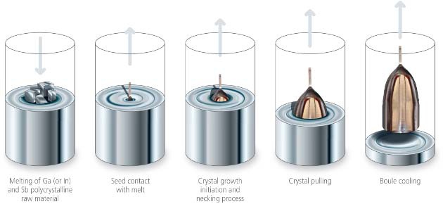
Figure 5. Simplified squeme of the Czochralsky method to produce single-crystalline silicon ingot (Figure credits: Galaxy Compund Semiconductors, Inc. www.galaxywafer.com/galaxy/technology/crystal-growth)
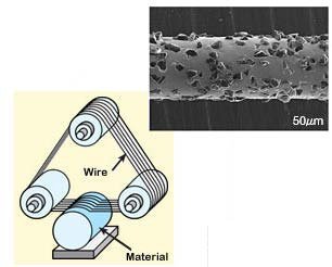
Figure 6. Basic scheme of a wire-saw machine used to slice ingots of a single-crystalline material, showing the microstructure of a wire (Figure adapted from: Ceratech Japan Co. Ltd, www.crtj.co.jp/e/cutting.html)
Final remarks
As final comments, it is important to point out that solar technologies are evolving so fast, that most experimental procedures and techniquescommonly used in the industrial production of wafers could seem obsolete. For example, in the case of purifying and refining silicon, I believe that hybrid techniques based on directional solidification/plasma refining, are to be the dominant in the industry. Another case to be mentioned is the crystallization of metallurgical-grade silicon. Although Czochralsky´s method is the most employed, modified versions have been recently proposed, such as the quasi-mono process, which involves a combination of Czochralsky´s method with ingot casting. Finally, the developing of more efficient cutting or slicing machines is taking a place in the state-of-art of wafering, since this can decrease the amount of material losses.
References
John Perlin, The Silicon Solar Cell Turns 50, NREL Report No. BR-520-33947, 2004
Lewis M. Fraas, Low-Cost Solar Electric Power, Springer, 2014
Gunnar Michelson, Solar Cell Array, United States Patent 3326497, 1967
H. W. Gillett, High Silicon Structural Steel, Technological Papers of the Bureau of Standards, No. 331, 1926
Ernest Braun, Stuart MacDonald. Revolution in Miniature: The History and Impact of Semiconductor Electronics, Cambridge University Press. 1982
Silicon Compounds – Advances in Research and applications, Scholarly Editions, Q. Ashton Acton Ed., Atlanta, Georgia, 2013
Stephen Malkin, Changsheng Guo. Grinding Technology: Theory and Application of Machining with Abrasives, Second Edition, Industrial Press Inc., New York, 2008
A. K. Lührs, W. Geurtsen. The application of silicon and silicates in dentistry: a review, Prog. Mol. Subcell. Biol., 47, 359-380, 2009.
B.S. Xakalashe, M. Tangstad. Silicon processing: from quartz to crystalline silicon solar cells, Southern African Pyrometallurgy, Edited by R.T. Jones & P. den Hoed, Southern African Institute of Mining and Metallurgy, Johannesburg, March 2011
S. Pizzini. Towards solar grade silicon: Challenges and benefits for low cost photovoltaics, Solar energy materials and solar cells 94, 1528-1533, 2010.
Jafar Safarian, Gabriella Trannel, Merete Tangstad. Processes for upgrading metallurgical grade silicon to solar grade silico, Energy Procedia 20, 88 – 97, 2012
Erwann Fourmond, Cyrille Ndzogha, David Pelletier, Yves Delannoy, Christian Trassy, et al. Refining of metallurgical silicon for crystalline solar cells, 19th European Photovoltaic Solar Energy Conference, 1017-1020, Paris, France. June 2004.
Excelente, ya comenzaste a publicar. Muchos éxitos.
Hola chama Emily...a ese ritmo primero me jubilan en URU...Saludos...
No te desesperes, estoy segura que tendrás mucho éxito en esta plataforma. Un abrazo