Everyday Electronics part #6: The Operational Amplifiers (Op-Amp)
Hello great steemians and welcome to this exciting series of everyday electronics and today, I will be taking us through a very interesting component in an analog circuit. I love solid state electronics and whenever the network of the data center I manage is not acting up, I love to get my hands dirty with soldering iron and some electronic component, and most times, I don't skip using OP AMP, as operational amplifiers are fondly called, in my little projects.

[Different commercial packaging of the operational amplifiers. Credit: Wikimedia. Creative Commons Attribution-Share Alike 3.0 Unported, 2.5 Generic, 2.0 Generic and 1.0 Generic license. Author: Omegatron]
Out of all the components I have reviewed in this series, this is the first active component I am reviewing and when we say a component is an active component, it means that the device or component has the ability to introduce a power gain in a circuit or produce some amplifications. An operational amplifier is an awesome electronic component in the sense that it can perform series of operations such as:
Clearly, Op amp earned its name; operational amplifier. The circuit symbol of the operational amplifier is a triangular shape with five terminals with the first two terminals being the input terminals with labels, positive and negative and two terminals in opposite side of the triangle vertex which corresponds to the positive and negative supply voltage and the last terminal, the signal output terminal. The output of the operational amplifier though single, is always relative the ground.
The output of the operational amplifiers depends largely on other components used alongside the op-amp itself and also depending on the configuration. Popular component used in conditioning the op-amp is the resistor and capacitor.
The Ideal Opamp
The characteristics of an ideal op-amp serves as a reference point for the real op-amp just like the ideal gas which is non existent helps us measure the performance of a real gas. The ideal op-amp does not exist in reality. The basic operation of the op-amp is to sense the difference in its input terminals, multiply this difference with latent gain "A" and produce the result of this multiplication as the output. This is why the input terminals of the operational amplifiers are called the differential input.
))
[the equivalent circuit of an ideal operational amplifier. Credit Wikimedia. Creative commons license. Author: Inductive load]
The first characteristic of the ideal opamp is unlimited input impedance. Impedance is the summation of resistance offered by a circuit. This input impedance is a measure of the ratio of input voltage to the input current. The input impedance is assumed or made to be infinite to ensure that no current flows into the amplifier from its input terminals though current still leaks from the input terminals of real operational amplifiers but this is only a few milliamps.
The second characteristics of an ideal opamp is zero output impedance. This is assumed to be zero because any operational amplifier should be able to be able to supply maximum current from the internal circuitry to the load thereby reflecting a perfect voltage source and zero internal resistance. Since the opamp has a single output, this output impedance is assumed to be in series with the load being driven by the amplifier, hence the opamp has a reduce output voltage. Real operational amplifiers have large output impedance usually above 100 ohms.
Another characteristic of the operational amplifier is an infinite open loop gain. An opamp is considered to be in an open loop configuration if it has no connection from the output to the input, this is called a feedback connection. Opamps are designed to amplify the signals applied to its input terminals and to do this, it need to have high open loop gain. Hence, opamps without feedbacks are assumed to have unlimited gain.
Finally, the ideal operational amplifier has an infinite bandwidth and zero offset voltage. Offset voltage is the voltage at the output of the amplifier when no voltage is applied to the input terminals. Hence, an ideal operational amplifier should have no voltage at the output when no voltage is applied at the input. Also the ideal opamp has unlimited frequency response, this makes it possible for the amplifier to amplify any frequency range be it at the AC or DC range, to any required frequency level. This is not the case for the real opamps as the bandwidth depends on a characteristic called gain-bandwidth product which I will discuss below.
The Gain-Bandwidth Product
As already stated above, the gain of any opamp is determined by its gain-bandwidth curve. Consider the gain-bandwidth curve shown, on the vertical axis we have the gain of the amplifier, which is the ratio of the input voltage or power to the output voltage or power, and on the horizontal axis we have the frequency of the amplifier.
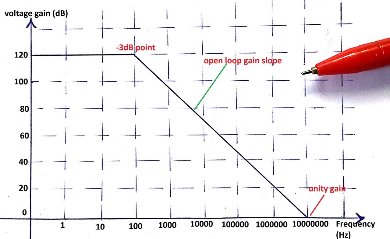
[Gain-Bandwidth product curve. Designed using windows paint and free hand by @henrychidiebere]
To facilitate understanding, I would like to summarize the graph before I even begin to explain the concept. The gain-bandwidth product curve shows that the cut off frequency of any operational amplifier is maximum when the gain is unity (1). Also an increase in the gain of any opamp results in a decrease in its cutoff frequency and it is impossible to amplify a signal beyond an amplifier's cutoff frequency.
Mathematically, the Gain-Bandwidth Product (GBP) is given as
GBP = Amplifier gain (A) * Amplifier bandwidth (Bw) = A * Bw
Also, xdB = 20 log (gain)
From the curve above, it can be seen that at a frequency of 100Hz, the gain of the amplifier is 80dB. To convert this value to a value multipliable by the frequency (the gain), we use above formula;
80dB = 20log (gain)
Gain (A) = antilog (80/20) = 10, 000.
Hence, GBP = A * Bw = 10, 000 * 100 = 1, 000, 000
Also from the curve, at frequency of 1000Hz, the voltage gain of the amplifier is 60dB, converting this to gain we have;
60dB = 20log (A)
A = antilog (60/20) = 1000
Hence, GBP = 1000 * 1000 = 1, 000, 000.
It can be seen that at any point on the curve, the GBP is constant (1000000). The gain bandwidth product helps us determine the possible bandwidth or gain of an opamp and this is determined by the unity gain (at 0dB).
Opamp Configurations
As already stated, the opamp has very wide range of applications and this all depends on the configuration of the the amplifier. In this section, I will discuss the widely used opamp configurations and their circuit diagram.
The Inverting operational amplifier
An ideal opamp has no connection between its output and input and this resulted in some assumptions which includes infinite open loop gain. Yes the gain of a real open loop opamp is very high, up to a million! But as good as this may sound, we are not in control of such gain, the open loop opamp is unstable making a little signal input would automatically saturate the output of the opamp.
))
[negative feedback configuration Wikimedia creative commons license. Author: Inductiveload]
To be able to control the gain of the amplifier, we sacrifice a part of the output signal by connecting the output signal to the inverting terminal (negative terminal) of the amplifier with a resistor controlling the amount of the output signal being sent to the input. The configuration of the inverting op amp is shown to the left, this connection from the output to the negative terminal of the amplifier is regarded as a negative feedback.
I = V/R but total voltage is given by Vin – Vout and total resistance = Rin + Rf
I = (Vin – Vout)/(Rin + Rf) let Vj = voltage at the feedback junction
Hence input current Iin = (Vin – Vj)/(Rin) = Vin/Rin – Vj/Rin
Output current Iout = (Vj – Vout)/Rf = Vj/Rf – Vout/Rf
Since the same current flows through the circuit, Iin = Iout
Hence, Vin/Rin – Vj/Rin = Vj/Rf – Vout/Rf making Vin/Rin the subject of the formula
Vin/Rin =Vj/Rin +Vj/Rf – Vout/Rf = Vj(1/Rin + 1/Rf) – Vout/Rf
But the inverting end is grounded, leaving Vj = 0
Hence Vin/Rin = -Vout/Rf rearranging this formular
Gain (A) = Vout/Vin = -Rf/Rin
By connecting a portion of the output signal to the inverting input, we have altered the original input voltage, hence the input signal at the inverting terminal now becomes a summation of the resultant negative feedback and the input voltage. To differentiate the input voltage from the voltage at the junction of the input voltage and feedback signal, we introduce the input resistor (Rin, shown in the image above).
Though the non inverting terminal (positive terminal) is connected to the ground, the voltage at the inverting terminal is equal to the voltage at the non inverting terminal. This is because, from the ideal opamp, there is an infinite input impedance making the potentials at both input terminals the same. But this has an implication; since the non inverting terminal is connected to the ground, a ground (called virtual earth) automatically exists at the point of connection between the feedback and the negative input terminal.
Due to this virtual earth at the feedback point, the input impedance of the amplifier becomes equal to input resistance making the gain of the negative amplifier to be determined by the ratio of the feedback resistor (Rf) and the input resistor (Rin). Mathematically (up left);
Clearly, the gain of the negative feedback opamp configuration can be controlled using two resistors, Rf and Rin. Hence, by making the input resistance very small and the feedback resistor very large, we can obtain an amplifier with a very high gain.
The non inverting Opamp
Though it might seem that the non-inverting configuration is the opposite of the inverting configuration but this is not true, in fact they produce gain that is in different sides of the number line. In this configuration, a portion of the output signal is fed back to the inverting input but this time, the non inverting terminal was not connected to the ground. The configuration of the non-inverting opamp configuration is shown below.

[A non-inverting configuration of the opamp. Credit: Wikimedia. Creative commons license. Author: Inductiveload]
As stated in the inverting configuration above, the voltage at both input terminals are equal and unlike the inverting configuration, the positive terminal is not connected to the ground. Since the same amount of voltage flows in the two input terminals, there is a voltage divider at the junction of the feedback resistor. Also the virtual earth still exists at the non-inverting terminal since the inverting terminal is connected to the ground.
The resultant voltage at the junction of the inverting input and the feedback point is given by the voltage divider formula and is given as;
Vj = R1/(R1 +R2) * Vout -----eqn (1) where Vj = voltage at the feedback junction
But from the ideal opamp, voltage at both terminals are equal hence;
Vj = Vin
And gain (A) = Vout/Vin; from equation 1
A = Vout/Vin = (R1 + R2)/R1 = 1 + R2/R1
From the formula above, one thing is very significant with the feedback loop of the non-inverting configuration, the gain will always be greater than or equal to 1. Also just like the negative feedback configuration, the gain is also controlled by the two resistors Rf which corresponds to R2 and Rin which corresponds to R1.
Theoretically, we can make the gain of the non-inverting configuration to be infinite by removing the input resistance but in reality, this gain limited by the amplifier’s default gain (open loop).
The differentiator
In order not to make this very blog to long, I will stop at the differentiator configuration but a grasp of this three different configuration I discussed ensures the understanding of the rest of the configurations as the rest are derived from these three configurations.
))
[differentiator configuration. Credit: Wikimedia Creative commons license. Author: Inductiveload]
One thing worthy of noting about the differentiator configuration is the output signal is equivalent to the first differential of the input signal.In this configuration, impedance has be substituted by reactance with the introduction of a capacitor, C. Also there is a negative feedback configuration as some portion of the output signal is fed back to the inverting input and the positive terminal is connected to the ground as shown in the image to the right.
Differentiation of the input signal occurs as a result of variation of the output voltage with respect to the variation of the input voltage with time. Hence, an increase in the input voltage will result in an increase in the input current and an even higher increase in the output voltage.
Capacitance, Q = C * Vin
Feedback current If = - Vout/Rf ----eqn 1
Since no current flows into the amplifier, Iin = If
Differentiating Q w.r.t we have
dQ/dt = C*dVin/dt
Also dQ/dt is equivalent to the input current, hence
Iin = If = CdVin/dt
From equation 1 feedback current If = -Vout/Rf, hence
-Vout/Rf = CdVin/dt
Therefore Vout = -Rf*CdVin/dt
The function of the capacitor is to drops all the direct current components of the applied voltage while allowing the alternate current component of the input voltage to flow, leaving no direct current at the feedback point of the amplifier. When the frequency of the input voltage is low, this causes a low gain of the amplifier due to very high capacitance.
On the other hand, when the capacitance, is very low (i.e, high frequence) the gain of the amplifier is so high that it becomes unstable and begin to oscillate which causes the output signal to saturate. To combat such situation, a second capacitor is placed in parallel with the feedback resistor. Mathematically (shown up left);
Apart from the instability issue pointed out earlier, the differentiator configuration is also prone to noise because of the input capacitance and since it has very high gain, this noise is easily amplified making the output signal almost unusable.
REFERENCES
- Operational amplifiers -electronics-tutorials
- Operational amplifiers-Wikipedia
- Introduction to operational amplifiers -sparkfun
- Opamps and its configurations -elprocus
- The differentiator -electronics-tutorials
If you write STEM (Science, Technology, Engineering, and Mathematics) related posts, consider joining #steemSTEM on steemit chat or discord here. If you are from Nigeria, you may want to include the #stemng tag in your post. You can visit this blog by @stemng for more details. You can also check this blog post by @steemstem here and this guidelines here for help on how to be a member of @steemstem. Please also check this blog post from @steemstem on proper use of images devoid of copyright issues here.

So have successfully decide to bring memories of the past..... EEE courses in school where not just fun for the mechanical guys but the end of the day it was fun
Good one boss... Lecture note in the making
You make rich content @henrychidiebere Thanks!!! All hails #steemSTEM :D
I really appreciate your time.
OP AMPs in my electronics class. this post refreshed my memory.