Methods of characterization of materials / part 9
Hello science-loving friends and welcome to my new installment of materials characterization, where I share my knowledge and experiences in the area of materials physics, especially semiconductor compound.
There are several publications that I have been writing during the last weeks concerning the electrical characterization of materials, which is divided in several sections due to the wide content.
There are different methods or experimental configurations that help us to know the physical and chemical properties of a semiconductor compound, some of these methods are well known to us and others perhaps not. During the last years, old techniques of characterization of materials have been created and perfected with the purpose of obtaining exact results in the measurements that help the scientists to simplify their studies and to be able to create technological tools that help to the advance of the same.
In my previous publications I have explained different experimental methods, mathematical developments that determine the most important electrical properties in a semiconductor such as "electrical resistivity", have basically the same purpose, which is to find mobility, the concentration of charge carriers of a material, where we involve different terms such as electrical conductivity, hall coefficient, energy gap, etc.
In this opportunity I will share the continuation of post #8 following the same trend, which is to study the electrical properties of the material using the "Van der Pauw" technique showing the definitions to obtain "Hall" measurements.
Before starting this eighth installment I recommend you to review my previous publications.
Here I will leave you the links:
Part 1 Part 2 Part 3 Part 4 Part 5 Part 6 Part 7 Part 8Let's remember the following:
Van der Pauw's technique is another used to find the electrical resistivity, mobility and concentration of charge carriers in a semiconductor material... It bears the name of its creator, and unlike the techniques explained above, "Van der Pauw" uses the surface resistance of the sample to determine the values of mobility and concentration in the material, remembering that in the first we use the hall coefficient and conductivity at room temperature.
This technique is used a lot due to its great advantages when it comes to obtaining viable results on the determination of important values such as measurements of the mobility of the load carriers at different temperatures, while in the previous one we can only do it at room temperature.
Now, we must remember that to make "Hall" measurements, we must be in the presence of a magnetic field, where we involve phenomenon such as the Lorentz force, which occurs when an electron circulates within the electric field perpendicular to the magnetic field being applied, therefore, this field experiences a force in both directions that moves constantly in response to the magnetic force and the force within the electric field of the material.
In this particular case I'm going to show you to determine Hall's measurements. If we know the thickness of the sample and the surface density of the charge and the volumetric density of the carriers, whether negative or positive, the Hall voltage in the sample can be very small, which brings great difficulty in obtaining satisfactory results due to the small magnitude that this voltage can present. Another important factor is the offset voltage caused by the placement of non-symmetrical contacts, the shape of the sample, and sometimes the non-uniformity of the temperature.
So how do we solve this problem?
The experts mention that you should have two sets of Hall measurements at hand so that each one has a function independent from the other, that is, one meter is in charge of taking data from the positive magnetic field and the other from the negative magnetic field.
The appropriate configuration for this measurement system is as follows:
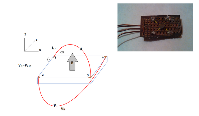
Configuration to determine the Hall voltage using the Van der Pauw
After preparing the sample correctly as shown in the diagram, the following definitions should be taken to perform Hall measurements:
Important note: the same procedure must be performed when the magnetic field B- is reversed (V24N, V42N, V13N and V31N ).
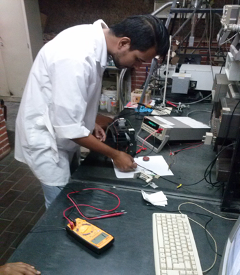
To start the Hall measurement process we must do the following:
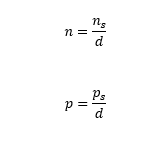
This procedure is interesting because the surface density of the material's load carriers can be determined ns as well as the type of sample (positive or negative), these data are essential in order to have a clearer idea of the technological application of such material. In turn, Hall mobility can be obtained by calculating ns y rs that we obtained in the electrical resistivity measurement shown in previous publications (that is why it is important to read my previous installments), however I will leave you with the equation below:
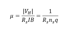
Note: for viable results. The above 8 measurements must be performed correctly as shown in each of the steps.
Mathematical calculations for Hall measurements:
To determine density and mobility, the following must be done:
VC = V24P - V24N, VD = V42P - V42N.
VE = V13P - V13N, VF = V31P - V31N.
if the sum of the voltages is positive.

if the sum of voltages is negative.

Where B is the magnetic field in gauss (G) and I is the direct current in amps (A).

END.....
The images are property of @carloserp-2000 and are for free use. For any extra information or questions you can leave your comment.
See you in the next installment where I will explain more about the electrical properties in a semiconductor.
Sources
Publish through our official app and you will get an extra vote of 5% https://www.steemstem.io/

 Video credits @gtg
This post has been voted on by the SteemSTEM curation team and voting trail. It is elligible for support from @curie and @minnowbooster.
If you appreciate the work we are doing, then consider supporting our witness @stem.witness. Additional witness support to the curie witness would be appreciated as well.
For additional information please join us on the SteemSTEM discord and to get to know the rest of the community!
Thanks for having used the steemstem.io app and included @steemstem in the list of beneficiaries of this post. This granted you a stronger support from SteemSTEM.