Methods of characterization of materials / eight part
Greetings from new science-loving friends and welcome to my new installment of materials characterization, where I share my knowledge and experiences in the area of materials physics, especially semiconductor compounds.
This would be publication number 8 concerning the electrical characterization of materials. I have decided to divide it into several sections due to the extensive content, since in order to study the electrical properties of a semiconductor material different experimental techniques are needed, some with which you feel familiar, especially chemists, physicists and engineers and others that perhaps had never been mentioned that are generally novel techniques which are based on old techniques already known. The ideal is to perfect each experimental method in order to obtain viable results in the measurements.

Before starting this eighth installment I recommend you to review my previous publications.
Here I will leave you the links:
Part 1 Part 2 Part 3 Part 4 Part 5 Part 6 Part 7In this installment I will continue with the development of Van der Pauw's technique explaining its experimental configuration, following by the analytical method to calculate the electrical resistivity in a semiconductor plate and some important tips to be able to obtain reliable measurements.
Let's remember that currently different techniques to calculate one of the properties in a semiconductor, such as "electrical resistivity", all have basically the same purpose, which is to find mobility, the concentration of charge carriers of a material, where we involve different terms such as electrical conductivity, hall coefficient, energy gap, and so on.
That is why this tool is fundamental for the creation of various optoelectronic devices and other technological applications, so it is important to study the physical properties of these materials and for this purpose different methods of experimental analysis are needed to give us results of its possible application in the technological field.
Van der Pauw's technique is another used to find the electrical resistivity, mobility and concentration of charge carriers in a semiconductor material... It bears the name of its creator, and unlike the techniques explained above, "Van der Pauw" uses the surface resistance of the sample to determine the values of mobility and concentration in the material, remembering that in the first we use the hall coefficient and conductivity at room temperature.
The main advantage of this technique is that it is possible to obtain mobility measurements of load carriers at different temperatures, while in the previous one we can only do it at room temperature.
Now, showing both diagrams of my previous publication and using the same configuration we can define the calculation of the measurement of electrical resistivity using the Van der Pauw technique.

Figure 1: Experimental configuration of the Van der Pauw technique for the determination of electrical resistivity in a semiconductor material

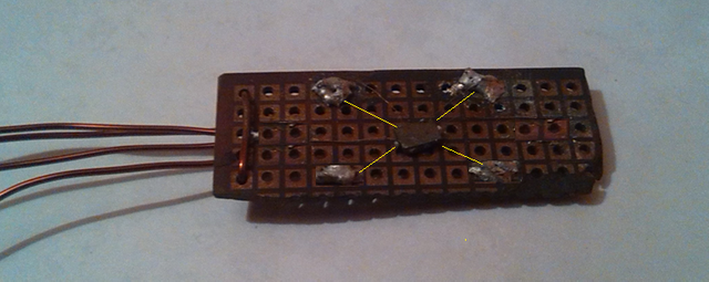
Figure 2: Real assembly of a semicondcutora sample
After preparing correctly the sample of the semiconductor material on the bakelite we proceed to connect the ohmic cables in the sample, these cables are preferably of very fine copper wire which adheres to the sample by means of a very small spot of tin solder. Label 1, 2, 3, and 4 counterclockwise as shown in Figure 1.
It is recommended to use the same quantity of copper wire for each contact in order to minimize the error of any thermolectric effect.
We must define certain very important parameters to perform the measurement process which are as follows:
ρ = electrical resistivity (at Ω-cm).
d = sample thickness (cm).
I12 = positive direct current enters into contact 1 and exits through contact 2. I23, I34, I41, I21, I14, I43, I32, I23 (in amperes, A).
V12 = direct current voltage measured between contacts 1 and 2 V1 - V2, without the applied magnetic field (B = 0). Equally for V23, V34, V41, V21, V14, V43 and V32 (in volts, V).

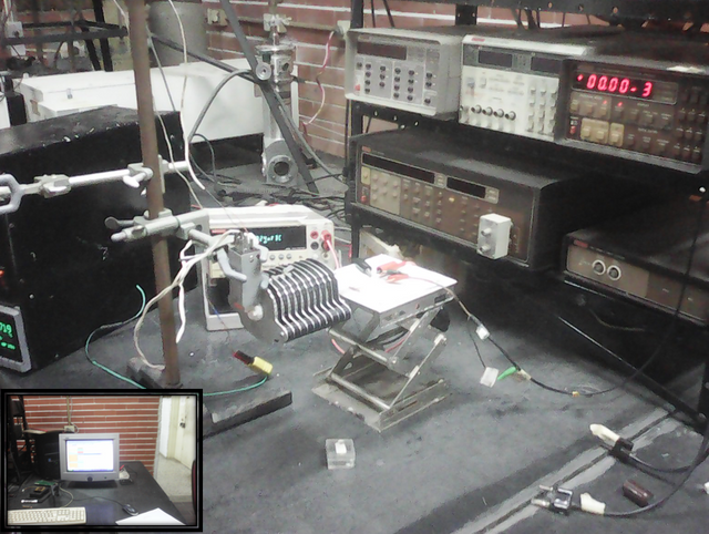
Figure 3: Real picture of the linear graph in the ohmic contacts of the sample
Before starting the measurement process, it is always recommended to check the ohmic contacts (current circulating linearly over the entire sample). The data must be verified for internal consistency, for the quality of the ohmic contact, and for the uniformity of the sample.
We prepare the direct current in the sample and have a range around 1mW. Then we measure the resistance in the material between any of the contacts, but these must be opposite, i.e. from contact 1 to 3 or from contact 2 to 4 and that I < (200R)-0.5.
Then we apply current in I21 and we measure the voltage in V34.
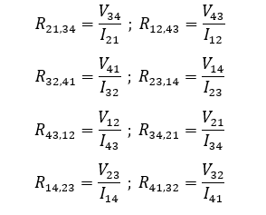
. We invert the polarity of the current in the semiconductor sample. I12 and we measure the voltage in V43. The procedure is repeated for the rest.In this step the voltage measurements produce 8 resistance values, which should always be positive and are as follows:


Important: When we perform the experimental configuration of the measurement system as shown in the previous image, we must take into account that the voltage meter only takes the positive voltages, therefore it must be set to zero subtly so as not to affect the system due to any sudden movement or external agent. In the same way the quality of the ohmic contacts play a fundamental role in the measurement and of course the uniformity of the sample.
The measures must be consistent and at the moment of reversing their polarity they must comply with the following condition:
R21,34 = R12,43
R43,12 = R34,21
R32,41 = R23,14
R14,23 = R41,32
Finally to perform the electrical resistivity calculations and determine the surface resistance which I explained in my previous publication the following is done:

Subsequently by means of the Van der Pauw equation described in my previous publication we solve:

If the thickness of the sample is known we can also determine the resistivity from:

Recommendation: In most cases when we practice this technique can present various errors in the measures, generally these errors can be caused to bad contacts, parasitic capacitances and non-uniformity of the sample. It is for that reason that it is necessary to check at every moment the assembly of the system of measurements and to verify the linearity of the current.
There may also be other effects that may distort the measurements which may be: Righi-Leduc effect, Seebeck, Peltier or Ettinghausen-Nernst. Also bad preparation of the sample, impurities, corrosion, bad positioning of the cables.
The images are property of @carloserp-2000 and are for free use. For any extra information or questions you can leave your comment.
See you in the next installment where I will explain more about the electrical properties in a semiconductor.
Sources
Publish through our official app and you will get an extra vote of 5% https://www.steemstem.io/

 Video credits @gtg
Hello,
Your post has been manually curated by a @stem.curate curator.
We are dedicated to supporting great content, like yours on the STEMGeeks tribe.
If you like what we are doing, please show your support as well by following our Steem Auto curation trail.
Please join us on discord.
This post has been voted on by the SteemSTEM curation team and voting trail. It is elligible for support from @curie and @minnowbooster.
If you appreciate the work we are doing, then consider supporting our witness @stem.witness. Additional witness support to the curie witness would be appreciated as well.
For additional information please join us on the SteemSTEM discord and to get to know the rest of the community!
Thanks for having used the steemstem.io app and included @steemstem in the list of beneficiaries of this post. This granted you a stronger support from SteemSTEM.