Methods of characterization of materials / fifth part
The characterization of semiconductor materials is a fundamental tool for the creation of various optoelectronic devices. During my stay at steem I have dedicated myself to sharing my experiences in this beautiful area of materials science. These experiences are based on the study of the physical and chemical properties of semiconductor compounds.
To make life easier, or rather to help people have a comfortable life, a lot of work is needed. By this I mean that before building a cell phone, television, solar panel or any electrical device it is necessary to start from the base, starting from all the theory involved, then following the experimental part where in principle we synthesize one or more elements of the periodic table and then create semiconductor ingots by means of the growth of synthesis.
Subsequently, the ingot must be conditioned according to the type of characterization to be performed, that is, we have different types of characterization (structural, electrical, optical, morphological) in each of them we have different analysis techniques where the sample must have different methods of preparation, either in ingot of different shapes and geometric sizes, wafer, thin film, dust, substance, etc.
After this step, the sample is prepared according to its technique and following the experimental configuration of the measuring equipment. In this case I personally have been sharing a series of articles related to the electrical characterization of materials from the preparation of the sample to its experimental assembly.
Then after experimentally configuring the measurement system and making the measurements, the results obtained from sweeping the sample must be analyzed and for this we need specialized programs where we raise the equations and obtain the results or simply do it manually, creating the method of analysis through the approach and solving the equations according to what we are searching for.

Previously we talked about the Hall effect and the importance it has in the characterization of semiconductor compounds, as well as calculating the Hall voltage in a semiconductor rod.
But before beginning to read this publication it is advisable to review the previous installments, in order to follow and understand the subject.
Here I will leave you the links:
In this installment we will focus on the calculation of the Hall coefficient, as well as which are the most appropriate methods to find this variable without errors. The concentration and density of the charge carriers in a semiconductor material and as a plus the energy gap.
There are different experimental assemblies for the measurements of electrical resistivity and Hall effect, some more efficient than others and some with a difference in cost. As I have just mentioned the technique of the Hall coefficient is very important for the study of semiconductors and that through this coefficient we can find the density and mobility of load carriers of the material, as well as the gap.
The most reliable experimental configuration to perform this type of measurements is the 6 contacts in my installment number 2 talk about how to prepare the sample for this experimental setup. Another experimental configuration is the 3 contacts in the center of the sample, however, this method is not very reliable, as it generates much difficulty when placing the contacts on the sample and consequently brings errors in the measurements. And another method is 5 contacts used by Dr Giovanni Marin in his undergraduate thesis in 1996[1].
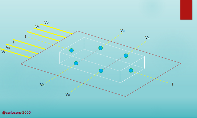
Diagram of the experimental configuration "6-contact method" for the calculation of electrical resistivity and Hall coefficient
In the previous image you can see how to configure or prepare the semiconductor sample and then proceed to its experimental assembly in the measuring equipment as shown below:
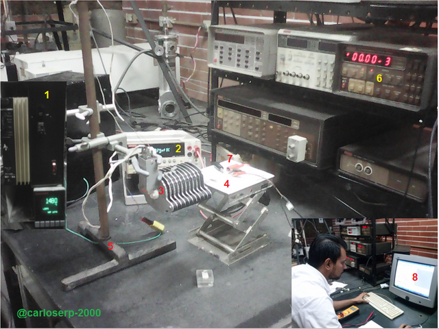
Actual experimental set-up of electrical resistivity measurements as a function of temperature
1. Temperature control.
2. Voltage source.
3. Oven.
4. Semiconductor.
5. Support.
6. Power supply.
7. Cables through which current and voltage circulate.
8. Software.
This image has been shown in previous publications, but it is important to show it again to keep track of the issue. In the image below we can see a real photo of the sample fully conditioned for measurement.
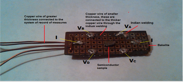
Real experimental assembly "method of 6 contacts" for the calculation of the electrical resistivity and Hall coefficient
Now, after having conditioned the sample and also having configured the experimental set-up to perform the measurements, we proceed to calculate the Hall coefficient by means of the voltage or the Hall voltage, by means of the following expression:

We can translate this as follows:
This is extremely important and we can demonstrate it by making a graph applying a general linear dependence of the voltage with the current, being α the proportionality factor, therefore, we define it in the following way:

Therefore,

In such a way that when assembling the graph of the Hall voltage in function of its current and applying a linear regression, we can obtain the value of α, and knowing each value of the thickness of the sample "d" and of course the magnetic field we can easily obtain the value of the coefficient Hall RH.

Example of a linear regression. CC BY-SA 3.0
On the other hand, by keeping the current constant, we can find a linear dependence of VH with B, bearing in mind that α is the proportionality factor.
Then with the factor α you have to,

Therefore,

In such a way that when assembling the graph of the Hall voltage in function of its magnetic field B and applying a linear regression, we can obtain the value of α, and knowing each value of the thickness of the sample "d" and of course of the current I we can easily obtain the value of the coefficient Hall RH.
Now, after obtaining the RH value we can calculate the mobility and density of the load carriers in the material.
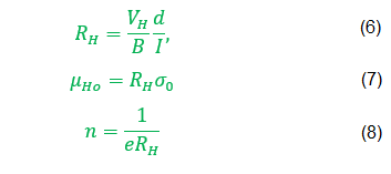
Where;
σ0 is conductivity at room temperature,
μ0 mobility of carriers at room temperature,
n the case of a carrier density.
If we know the diameter of the semiconductor sample, we can calculate this conductivity, and the resistance can be obtained from the following expression:

We can obtain μH0 through the following equation:

The concentration of the charge carriers n (hollows-electrons) in the semiconductor sample is given by:

This resistivity method has a great advantage due to its versatility, i.e. apart from being able to calculate electrical parameters such as density, mobility, conductivity and concentration of load carriers in a semiconductor material, it also has the capacity to obtain the value of the energy gap or the Eg gap.
Usually this type of measurements are made by optical characterization of a semiconductor material, as it provides us with specific and 100% reliable values of the sample. But this resistivity method is very useful when you only want to work with electrical characterization and this calculation would be a very important plus in our study if we want to advance much further.
Then, from the calculation of the conductivity of the temperature reciprocal we can define it in the following way:

V= voltage,
l= length of the semiconductor sample,
A= cross section,
I= current and
ρ= resistivity.
To determine the conductivity of a semiconductor 3 types of measurements are used:
Characterization at low temperatures, in this by the effect of temperature the carriers are activated and the conductivity tends to grow linearly, usually this is done with extrinsic semiconductors, ie containing some degree of impurities in the material or are doped.
Characterization in high temperatures, quite the opposite, to the previous one. In this case we have a pure semiconductor without presenting impurities, the load carriers of the material are transferred from one band to another (valence to conduction), due to the high temperatures supplied. Here the graph is described exponentially.
Characterization at medium temperatures, where vacuum of impurities occurs, since a later temperature increase no longer produces an activation of the charge carriers of the impurities.
In this case we follow the method of high temperatures through the following expression:

where,
σ0: is the electrical conductivity at room temperature,
Eg: energy gap,
T:: temperature and
KB: This is the Boltzmann constant.
To calculate the energy gap we must have the logarithm of the equation:

In this case we must represent Lnσ by means of a graph y=Lnσ ; x=1/T and obtain a linear equation of the form y=a+bx, and the slope of this line is given in the following way:

And by linear regression we finally get the equation to calculate the energy gap by electrical characterization of a semiconductor:

Conclusions
In this publication we have just demonstrated the importance of the Hall coefficient method for the electrical characterization of a semiconductor material. Mobility, concentration, conductivity and density are very important studies for these materials, as they tell us what their physical behaviour is. Besides, the Hall effect is important because it allows by means of a practical method to know if a sample is type p o n and thus to be able to determine the concentration of its charge carriers (hollow electrons).
An important feature in the study of semiconductors is the mobility of charge carriers as it allows us to measure the ability of the carrier to move under the action of an electric field, is undoubtedly one of the most important parameters that are related to the transport of semiconductors.
And finally, calculating the gap by electrical measurements and as long as it is done according to its temperature, is another fundamental parameter. It allows us to accurately calculate the value in emV of how much energy is needed to break this gap, ie move from one level to another (valence-driving).
And what is this needed for?
The answer is simple...Thanks to this we can know that semiconductor material is a candidate to be a prototype in the manufacture of solar cells.
Sources
Publish through our official app and you will get an extra vote of 5% https://www.steemstem.io/

 Video credits @gtg