Methods of characterization of materials / Second part
The electrical resistivity "ρ" is a magnitude that characterizes the difficulty that a specific material opposes to the flow of charge carriers. It is also known as one of the most sensitive indicators of changes in the nature of chemical bonds. In general, the electrical resistivity is inversely proportional to the density of the carriers and to the mobility of the carriers. A change in the nature of the chemical bonds would mainly alter the density of the carriers, and the structural changes would alter the mobility of the carriers. Experimentally, the electrical resistivity in metals increases approximately by a factor of 2 at the melting point, while in semiconductors like silicon and germanium it decreases when they are transformed from solids to liquids.
On the other hand, the electrical conductivity "σ", which describes the electric current density "J" produced in a solid by an electric field "E", is the inverse relationship of the electrical resistivity.
Conductivity theory explains the following experimental observations:
In many solids σ is independent of the field by moderate field strengths. The current density and the field are described linearly by Ohm's Law.
Different solids may have very different conductivities. In metals, σ is of the order of 106 (Ωcm)-1, however, in semiconductors σ it covers a range of 15 to 20 orders of magnitude below the previous value.
There is a big difference in the dependence of σ on metals and semiconductors. In a wide temperature range, for metals σ is proportional to T (- 1). At low temperatures, simple metals show a dependence on T (- 5). For intrinsic semiconductors, σ follows an exponential dependence with exp (- α) /T). This temperature behavior describes samples without imperfections in the network. This leads to differentiate the dependence of the temperature of the electrical conductivity of the semiconductors on the metals in all the temperature range.
Later I will explain the concentration of charge carriers in semiconductors, electrical conductivity and all the equations involved to calculate this type of physical property in these compounds.
Now, we will focus on explaining the method of 6 contact bars, this method is important to calculate the mobility and concentration of charge carriers, always depending on their temperature.
Previously, we said that electrical conductivity is one of the most important physical properties in a solid material. Since it can provide us with information about the concentration of load carriers and mobility of these, the purpose of being able to obtain this type of analysis is without a doubt to be able to observe the behavior of the material and if it can be applied in a field in specific, with this I mean in the manufacture of any technological device.
There are two experiments that can provide this information, in fact they are relatively easy, one of them is the electrical resistivity measurements and the other the Hall effect. These experiments give us information about the activation energy and the concentration of the major charge carriers (electrons, type n, holes, type p). As I mentioned in the previous post, you must have a semiconductor bar to which you must make electrical contacts with a very fine copper wire and then make an impact current (I).
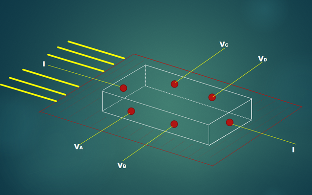
Diagram of the semiconductor bar placed on the bakelite with its respective copper wires that indicate the circulation of the current
As you can see in the diagram above, the difference with respect to the previous characterization method is the connection of two cables that indicate the voltage, the purpose is to be able to perform Hall effect measurements.
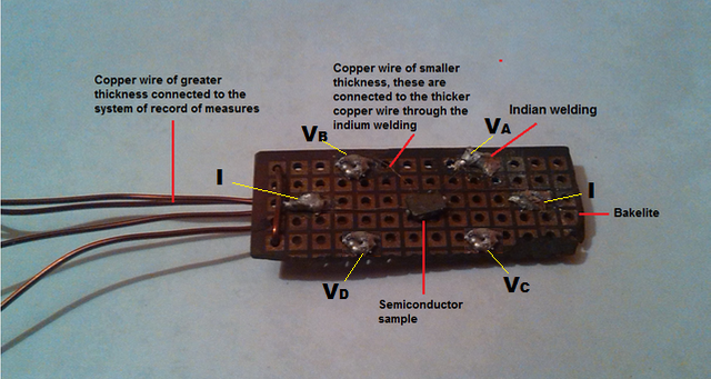
Real assembly of the semiconductor bar placed in bakelite for the electrical resistivity and hall effect measurements.
It is important to note that the sample of the semiconductor material that is to be characterized by means of this experimental method must have certain considerations regarding its size, for example the material shown in the photo has a diameter of 1.5cm in length, 0.75. cm wide and 0.20cm high. This also brings certain limitations at the time of assembly since it is quite difficult to work with samples of this size, it is advisable to work with a microscope to be able to observe in detail when making contacts on the sample.
Another extremely important detail is that if the contacts are not perfectly aligned to match the opposite ends of the same equipotential line, this would result in errors in the measurements.
The following image shows how the contacts should be perfectly aligned (parallel to each other).
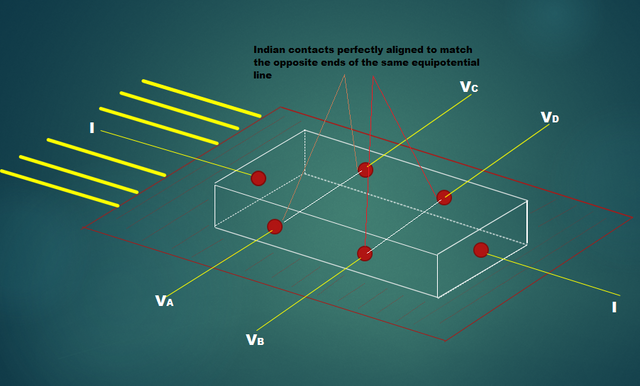
Diagram showing the indian contacts perfectly aligned to coincide with the opposite ends of the same equipotential line
Then, to calculate the electrical resistivity in a semiconductor bar using the method of 6 contacts or points the following equation is used:
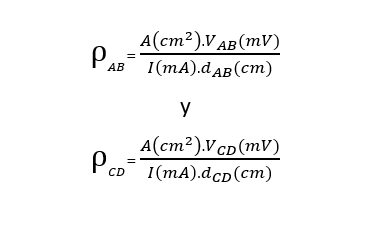
where VAB and VCD is the difference of electric potential between the points AB and CD, dAB and dCD is the distance between them and A the transversal area of the sample. In addition, this measure provides information on the homogeneity of the material when comparing the values of ρAB and ρCD should be similar in magnitude.
The Hall voltage is calculated by the following expression;

It should be mentioned that these calculations must be carried out in the same way for the CD contacts, the + and - signs that are inside the parenthesis describe the conditions of the magnetic field and the direction by which the current flows within the system.
After having calculated the Hall voltage, we can calculate the concentration of the charge carriers in the semiconductor bar through the following equation:

where I is the current, B is the magnetic field, l is the thickness of the sample and e is the charge of the free carrier.
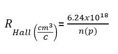
Finally, in a special case where the charge carriers are electrons (n) or holes (p), the respective expression is:
And this is all for this occasion, friends. In next installments I will continue explaining more about the electrical properties of semiconductors and different methods of characterization of materials.
If you want more information about the subject you can visit the following links:
Electrical resistivity and conductivity Semiconductor Basics Resistivity Measurement of Semiconductor ParametersPublish through our official app and you will get an extra vote of 5% https://www.steemstem.io/

 Video credits @gtg
Hola @carloserp-2000
El tema de la física no es mi "plato fuerte", pero aun así leí y vote por tu artículo porque me llamó la atención todas las imágenes. ¡Están nítidas y bien presentadas!
Disculpa que utilice este medio para comunicar que entre al Discord y no encontré ninguno de mis servidores (steemstem, steem-espanol, ni el de cervantes). Aun no entiendo que pasó... ¿Será que me ausenté demasiado y perdí la oportunidad de seguir compartiendo con ustedes por ese canal?
Saludos!
Saludos servidor de steemSTEM https://discord.gg/edxs53S
Servidor de STEM-Espanol https://discord.gg/Fef7p2m
Gracias!
This post has been voted on by the SteemSTEM curation team and voting trail. It is elligible for support from @utopian-io.
If you appreciate the work we are doing, then consider supporting our witness stem.witness. Additional witness support to the utopian-io witness would be appreciated as well.
For additional information please join us on the SteemSTEM discord and to get to know the rest of the community!
Thanks for having added @steemstem as a beneficiary to your post. This granted you a stronger support from SteemSTEM.
Thanks for having used the steemstem.io app. You got a stronger support!
Hi @carloserp-2000!
Your post was upvoted by Utopian.io in cooperation with @steemstem - supporting knowledge, innovation and technological advancement on the Steem Blockchain.
Contribute to Open Source with utopian.io
Learn how to contribute on our website and join the new open source economy.
Want to chat? Join the Utopian Community on Discord https://discord.gg/h52nFrV