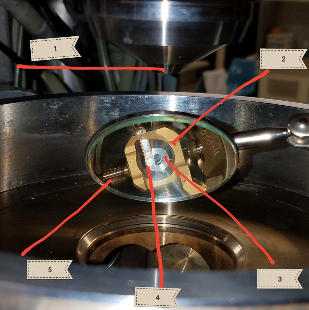
Inside the stage of a 0.22 nanometer resolution Transmission Electron Microscope
Shown here is the specimen stage for Philips CM 30 TEM. It has an accelerating voltage of 300kV and can resolve 0.22nm (2.2 Angstrom). Generally speaking, the higher the voltage, the smaller details you can see. Their is an upward limit however, but that is another story.
- Upper Objective Pole Piece.
- Anti-contamination device
- Lower Objective pole piece. The two pole pieces are part of the Donut shaped Objective Lens assembly, which focuses the electron beam, along with several other electromagnetic lenses to create a high resolution image.
- Removable Objective Apertures (4 of them, and moved out of beam path). Apertures essentially reduce aberrations.
- Left translator bushing aka specimen manipulator.
At this time the specimen is not inserted, but it would be right above the lower pole piece. The specimen holder secures a 3 mm diameter, very thin, ablated material or a grid that the sample is applied to using a variety of methods depending on substance. In TEMs the beam is passed right thru the specimen, unlike Scanning Electron Microscopes it is deflected off the surface. The final destination of the electrons in either type is a transducer. The case of a TEM the transducer is a or a Phosphor screen, or Scintillator coupled to a digital camera.
I took this picture while inspecting the stage area, which is extremely delicate and under very high vacuum when up to parr.

Interesting
I will follow you to see your future posts!