Everyday Electronics part #7: Field Effect Transistors (FETS)
Good day everyone and welcome to yet another interesting version of everyday electronics and today I will be talking about the field effect transistors, their mode of operation, how to recognize them, their applications and how to work with them.
My first experience with the field effect transistor was not really a good one. As a university student struggling with funds, I had an inverter project at hand (the first inverter I designed and implemented). As already stated, my funds were highly limited, hence, I bought all the components without making space for exigences (which was very unprofessional). Well, the transformer was ready, the charging circuit was also ready, in fact everything was ready except for the MOSFET (a type of FET) line which I thought was the simplest to implement as it only entails soldering it on the board and fastening it to a heat sink.
[Credit: Wikimedia. Creative Commons Attribution-Share Alike 3.0 Unported license. Authour: unknown]
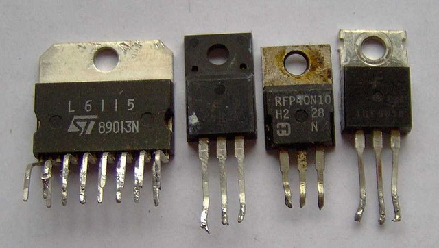
Ladies and gentlemen, I soldered everything to the circuit board and designed a very nice heat sink for my MOSFET line which will do the major work of DC to AC conversion (Pulse width modulation). On powering my circuit, only the fan was rotating every other component was dead silent. Well, to cut the whole story short, I discovered my MOSFET was not functional. Why? I spent a considerable amount of time soldering them and the little heat from the soldering and its output pins destroyed the component. That was when I realized that the MOSFET was actually one of the costliest component in my circuit cause I had about 7 pairs with each costing $2.4.
What is a Field Effect Transistor?
))
Composition of "normal" transistor (BJT). Creadit: Wikimedia. Creative commons license. Author: inductiveload]
I've discussed about diodes, transistors and operational amplifiers in this series and the knowledge of the three will help us understand and appreciate FET transistors better. The transistor I discussed about which has three terminals; Emitter, Base and Collector, are known as Bipolar Junction Transistors (BJTs). They're known as the "ordinary" transistors and their operations are based on normal semiconductor principles (holes and electrons). The operations of the BJTs are controlled by the holes and electrons which are the two charge carriers and hence their name, "bipolar".
Field Effect Transistors are "Unipolar" transistors, which means their operations are controlled by just one carrier. The operations of the FET are controlled singly by the Electric field, hence they are also a voltage controlled device. The major drawback of the normal transistor is that it have small input impedance. One of the qualities of an ideal operational amplifiers is that it have infinite input impedance though in reality, this only means their input resistance are very high. FETs beats the BJTs in this respect with their input impedance being considerably high.
[Analogy of operation of FETs. Credit: Wikimedia. Creative Commons Attribution-Share Alike 2.0 Germany license. Author: Stefan Riepl]
Another drawback of the BJT is that it has a great deal of noise when compared to the FETs. The FET is a three terminal device which are Gate, Source and the Drain. As already stated, the FETs are controlled by a single charge carrier which is either the hole or electron. In the P-channel FETs, the charge carrier is the holes while in the N-channel FETs, the charge carriers is the electrons. Because of the high input impedance, the field effect transistors makes a better amplifier than the bipolar junction transistors.
It consists of four (4) terminals when the not so popular body terminal is included. The Gate terminal functions by creating an electron channel between the drain and the source terminal thereby by allowing or limiting the passage of electrons, hence its name Gate. The source terminal is the entry point of charge carriers into the channel, just as the name implies. The amount of current entering the channel through the source is called the source current (Is). The drain terminal acts as an exit path for the charge carriers.
There are many types of the field effect transistors but the basic type only includes the Metal Oxide Semiconductor Field Effect Transistor (MOSFET) and Junction Field Effect Transistor (JFET). The working principle of these two field effect transistors will to a great extent explain the basic working principle of other types of FETs.
The MOSFETs
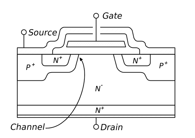
MOSFET was the first and only field effect transistor I have used in the field and is also the most widely used field effect transistor due to its impressive performance in switching and amplifications. MOSFET is also called the insulated gate FET because the gate is insulated from the dielectric layer of silicon oxide (SiO2).It is purely a voltage controlled device whereby the applied voltage controls the conductivity of channel between the source and the drain. The MOSFET consist of four terminals which are; Source, Drain, Substrate or body and Gate, abbreviated S, D, B and G respectively.
))
[A P-channel MOSFET. Credit: Wikimedia CC3.0 license. Author: Markus A. Hennig]
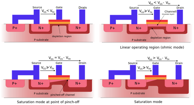
Just like the general FETs, carrier charges finds their way into the channel through the source and exits through the drain. Voltage applied at the gate determines the width of the channel. MOSFETs are basically of two types which are Depletion type and Enhancement type. The depletion type can be seen as a normally open switch whereby an applied voltage at the gate is required to close the channel while the enhancement type can be seen as a normally closed switch whereby an applied voltage at the gate is required to open the channel.
Principle of Operation
The most important part of the MOSFET is the MOS capacitor which is formed by three bodies, the body/substrate, the silicon oxide insulation and the metal electrode at the gate. The conductivity of the channel which summarizes the operation of the MOSFET is determined by this MOS capacitor. The application of either positive voltage or negative voltage at the gate can make the semiconductor located just below the oxide become either a P-type or an N-type. Depending on the construction, MOSFETs are classified into:
- N-channel MOSFETs and
- P-channel MOSFETs
))
In the P-channel MOSFET, the gate (G) and the Source (S) region are doped heavily with a P-type material while the body or the substrate is doped with an N-type material. The principle of like charges repelling each other is applied in the design of both the n-channel and the p-channel MOSFET. When we apply negative voltage at the gate, the region which is just below the silicon oxide dielectric material consists of a negatively doped substrate, hence the electrons at this region is literarily pushed further downwards towards the body thereby creating a channel.
The already depleted electron region is then occupied by positive charges (holes) from the highly doped source and drain region. Also the creation of the channel is aided by the fact that the electron will further attract the holes towards itself.
[An N-channel MOSFET. Credit: Wikimedia. CC1.2 license. Author: CyrilB]
In N-channel MOSFET, the reverse is the case here. The source and the drain are highly doped with a negative type material while the substrate/body is doped with a positive type material. Unlike the P-channel MOSFET, the conductivity provided by the channel is due to the flow electrons.
Here, when positive voltage source is connected to the gate, the positively charged gate forces the positively charged holes which exists just below the silicon oxide layer to move further to the substrate since they are like charges. The displacement of the holes creates a depleted region which is quickly occupied by the electrons from the two electrodes (source and the drain). The creation of the channel is further enhanced by the attraction forces of the electrons.
The JFETs
The junction field effect semiconductor is similar to the MOSFET in the sense that both are voltage controlled and movement of current is as a result of a single charge carrier; either hole or electron. It is also characterized by very high input impedance making it also a good candidate for amplifier applications. Compared to MOSFETs, the JFETs could be viewed as cheap component and can be considered in amplifier projects where cost is of concern.
))
[JFET symbol. Credit: credit: wikimedia. Creative Commons Attribution-Share Alike 4.0 International, 3.0 Unported, 2.5 Generic, 2.0 Generic and 1.0 Generic license. Author: Zedh]
))
[MOSFET symbol. Credit: Wikipedia. Creative Commons Attribution-Share Alike 2.5 Generic License. Author: Wojciech_mula]
The symbol of JFET is quite different from that of MOSFET and unlike MOSFETs, it consists of three terminals which are Source, Gate and Drain. The operation of the JFET is more straightforward when compared to that of MOSFET and can be viewed as device consisting of a channel and a central diode in a reverse biased mode. The operations of the terminal is similar to that of the MOSFETs and the voltage at the gate also controls the flow of current through a channel created between the source and the drain.
Principle of Operation
The JFET Consists of a bar which could be of P-type material or an N-type material. The bar consists of doped silicon or gallium arsenic compound. The gate which is between the source and the drain is insulated from a heavily doped P-type material or N-type material. Unlike the MOSFET, the gate exists at the two sides of the bar and is responsible for setting up or tearing down channel between the source and the drain.
[different operating region of the JFETs. Image credit: Wikimedia. Creative Commons Attribution-Share Alike 3.0 Unported license. Authors: Olivier Deleage and Peter Scott
_Cross-section.svg)
.svg)
Unlike the MOSFETs which can be either normally open or normally closed as described above, the JFET is only in one mode, normally open (which is one of the major reason is not widely used) and the channel is formed to block the electron or hole from conducting current through the bar. Hence, the channel can be likened to a voltage controlled variable resistor whereby in the absence of voltage at the gate, maximum current is allowed to flow through the bar and as voltage is applied at the gate, a resistive channel is formed starting from both ends of the gate and depending on the magnitude of the applied voltage at the gate, the channel can extend at both ends thereby totally blocking the current flowing through the bar.
Since the gate region is highly doped, some part of this region will diffuse into the bar forming a little depletion region. There are basically two classes of JFETs which are:
- N-channel JFETs and
- P-channel JFETs
In the N-channel JFETs, the bar is made up of a conductive N-type semiconductor material. As already stated, the gate exists at both ends of this bar but the regions of these gate terminals are doped highly with a P-type material. These highly doped regions, the source and the drain are terminated with an ohmic contact. The two highly doped positively charged region and the negatively charged bar forms an P-N junction, hence the name, junction FETs. This P-N junction is formed by the diffused portion of the highly doped gate region in the bar.
))
[An N-channel JFET with a negative bias voltage. Credit: Wikimedia. Creative Commons Attribution-Share Alike 3.0 Unported, 2.5 Generic, 2.0 Generic and 1.0 Generic license. Author: Armael]
Biasing the N-Channel JFET is different from that of MOSFET, this is because, and only negative voltage is applied to control the gate. Applying positive voltage to the gate will result in the damage of the device because a positive gate voltage will channel all the current in the bar to the gate. Voltage applied between the gate and the source which controls the channel is called VGS(gate to source voltage) while voltage across the drain and the source is called VDS (Drain to source voltage).
The conductivity of the channel is dependent on the width of the depletion region. When VGS = 0, the width of this depleted region which exists at both sides of the bar is high in the region between the drain and the gate than in the region between the gate and the source. With no voltage applied at the gate, maximum current flows in the channel, this current is known as the drain current.
When negative VGS is applied at the gate and the source, this results in an increase in the depletion region within the bar thereby reducing the width of the bar and subsequently, the drain current Id. This is known as reverse biasing of the JFET and generally, all JFET are reverse biased.
As the negative VGS increases (negatively), so also the depletion region and a point will reach when the depletion region at both ends of the gate will come together and completely block the flow of current through the channel. This is known Pinch-Off point of the JFET and the value of the negative gate voltage at which this pinch-off occurred is known as Pinch-off voltage.
The reverse is the case for the P-channel JFET. Here, the channel is made of P-type material and the gate region is highly doped with N-type material which diffuses into the channel creating a depletion region. The biasing of the P-channel JFET is the same with that of N-channel just that here, positive voltage (+VGS) is applied at the gate. As value of VGS is increase, the conductivity of the channel is reduced thereby limiting its conductivity. Pinch-Off state is reached when the channel is completely blocked by the depletion region.
Application and Summary
Field effect transistors are unipolar devices which means that the flow of current is as a result of one charge carrier in contrast with the bipolar junction transistors where the flow of current is as a result of both holes and electrons. They are also voltage controlled device and consists broadly of Junction Field Effect Transistors and Metal Oxide Field Effect transistors. JFETs are three terminal devices which are always in reverse biased mode and also considered as normally open device irrespective of its classification and configuration. The MOSFETs can be normally open or normally closed and are the most widely used FETs.
FETs are extremely fast switching device, faster than normal transistors. The advent of FETs made the dreams of every IC fabricator come true. One of the widely used transistors in digital logic chips is the complementary metal oxide semiconductor (CMOS) which can be miniaturized and consume very low power. FETs also handles heats better than bipolar junction transistors. FETs are better amplifiers than BJTs because it can completely isolate input current from operating current due to its high input impedance and zero offset voltage.
REFERENCES
- Field Effect Transistor Circuit, Basics and Characteristics -efxkits
- Field effect transistor -Wikipedia
- Types of FETs and their working principle -elprocus
- Construction and working principle of JFETs -electronicspost
- MOSFET -wikipedia
If you write STEM (Science, Technology, Engineering, and Mathematics) related posts, consider joining #steemSTEM on steemit chat or discord here. If you are from Nigeria, you may want to include the #stemng tag in your post. You can visit this blog by @stemng for more details. You can also check this blog post by @steemstem here and this guidelines here for help on how to be a member of @steemstem. Please also check this blog post from @steemstem on proper use of images devoid of copyright issues here.

Your post has just been upvoted by the steemjet community. We support creative talents with upvotes too
Hi @henrychidiebere!
Your post was upvoted by utopian.io in cooperation with steemstem - supporting knowledge, innovation and technological advancement on the Steem Blockchain.
Contribute to Open Source with utopian.io
Learn how to contribute on our website and join the new open source economy.
Want to chat? Join the Utopian Community on Discord https://discord.gg/h52nFrV
This post reminds me of my final year project
Great work man ....i look forward to reading your next posts @henrychidiebere
you know this inec batteries right? That adapter is uses to connect to a laptop and charge it what kind of conversion happens in there am just wondering cos it's kinda difficult to find if you wanna buy it