Electron Beam Lithography - A Brief Review
Since the late 1980s, electron beam lithography has been a topic of great interest in the field of nanoscience, in part due to the lucrative opportunities for commercial application. There is high demand for improved nanoscale materials with increasingly complex tractable patterns in the rapidly developing microprocessor sector. Other applications, pursued in academia include the patterning of magnetic materials and the development of ultra-fast systems, which hold great promise for the development of improved of low dimensional semiconductor devices and novel applications.
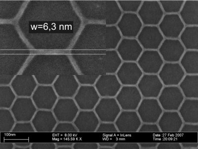
Fig. 1: Honeycomb pattern, defined by electron beam lithography and etched into the ferromagnetic semiconductor GaMnAs with 6nm wide semiconductor bars, shows the ultimate potential of top down patterning techniques. Such ultra small structures are used to probe interference phenomena of charge carriers in ferromagnetic semiconductors. Reproduced from goo.gl/56mqRY.
I. Introduction
Electron beam lithography (EBL), as described by McCord and Rooks (2000), is the name for the ubiquitous process in nanotechnology in which fine patterns are embedded in an electron-sensitive film on a surface, commonly referred to as a resist. This is achieved by subjecting the surface to a focused beam of electrons, the effect of which is to change the solubility of the resist according to (Owen and Rissman, 1983)
where S0 is the solubility of the unexposed resist, E is the absorbed energy density at the resist cell, E0 is the threshold level of energy density at the resist cell, and alpha is a measure of resist contrast. As the solubility of the surface is subject to variation through this process, selective removal of the exposed, or non-exposed regions of the resist is made possible via immersion in an appropriate solvent. This flavour of EBL is known as projection printing (Tseng et al., 2003), and is one of two distinct schemes.
The other main strategy in EBL is known as direct writing. It is usually the case that a finely focused (Gaussian) round beam is used, with raster scanning employed while the beam is made to move with the sample so that pixels are exposed one-by-one. Direct-write EBL is often favoured over project printing EBL in cases where the generation of maximally fine patterns is of greatest priority (Broers et al., 1996).
The overarching purpose of EBL techniques is to generate nano-scale structures in the resist so that the pattern may be delegated to the substrate. The most common process by which the resist pattern is transferred to the substrate is etching (Brewer, 2012). The chief advantage of direct-write EBL is that it facilitates the generation of tractable patterns, with resolution below 10nm(Vieu et al., 2000). This form of high resolution lithography is referred to as maskless (Menon et al., 2005), and is coupled with low throughput which, as outlined by Tseng et al. (2003), limits its application to that of low production semiconductor devices and photomask production. For details on photomask etching, refer to the excellent review by Wu (2006).
II. Procedure and System
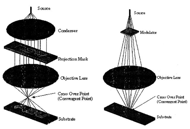
The general operational schematic for direct writing and projecting printing EBL system is illustrated in Figure 2. Written directly onto the resist-coated substrate is an ultra-fine topographical point provided by the electron beam in the direct writing regime. As a direct result of this, the need for masks is eliminated, which can be considered an advantage given the challenges that their production poses, as outlined by Liddle et al. (1991). A high precision lens system is implemented in the general projection printing system, the purpose of which is to project the (rather large) electron-beam pattern parallel through the mask to meet the substrate. Parker et al. (2000) put forward the minimum electron beam write time; that is, the minimum time necessary in the exposition of a given area for a given dose as
where T is the time to expose the object, I is the beam current, D is the dose and A is the area exposed to the beam. It is the case that average beam write times are far beyond optimal levels for large scale implementation in industry, and as such alternative lithographic processes are often used.
FIG. 2: Schematic of direct writing and projection printing systems, reproduced from Tseng et al. (2003).
As noted by Tseng et al. (2003), Bell Laboratories were the first to design and implement a projection EBL system, with the invention of the Scattering with angular limitation in projection electron-beam lithography (SCALPEL) system (Berger and Gibson, 1990). Further noted by Tseng et al. (2003); IBM developed the projection reduction exposure with variable axis immersion lenses (PRE-VAIL) during the 1980s with the development of the variable axis lens for EBL systems (Pfeiffer, 1992, 2000). In recent years, with the advent of sub-10nm resolutions, cutting-edge fabrication tools have been developed (Gangnaik et al., 2017), however the maximum output efficiency of this technology is limited not exclusively limited by the semiconductor length scale. Indeed,the maximal output potential of this technology is also limited by the substrate and resist-materials, the processes of the pre/post-fabrication treatment, etc.
III. Future Challenges
A. Resist Development
Due to the relative low mass of electrons, it is the case that the focused beam used in EBL processes cannot engrave substrates composed of typical materials. Resists, therefore, are a focal area of research, upon which the development of EBL processes is dependent. Fabrication processes are the mechanism by which the engraved pattern is transferred to the surface of the substrate. The most commonly used resists, such as PMMA (Polymethyl-methacrylate), ZEP (Nippon Zeon) and HSQ (Hydrogen Silsesquioxane) are ubiquitous as a result of their maximal lithographic outputs (Gangnaik et al., 2017). It was demonstrated by Yang et al. (2009) that HSQ resists provide the highest resolution lithographic outputs, at length scales below 5nm. The logistical challenges coupled with HSQ resists, however, are thelimited shelf-life (up to 6 months) and the requirement that it should be stored in ambient conditions of 5 degC. Such requirements, along with the fact that HSQ is subject to cross-linking when exposed to moisture (Häffner et al., 2007) contribute to the challenges of large scale implementation.
PMMA is a widely used resist, exhibiting greater sensitivity than HSQ, but to a lesser degree than the relatively emerging ZEP, which was first manufactured in the late 1980s (Tanenbaum et al., 1996). Various EBL fabrication techniques have been established utilising PMMA of varying molecular weights, and a number of sub-10nm resolution structures have been established through its implementation (usually with low temperature and high electron beam voltages) (Yasin et al., 2002). Resists are broadly categorised into positive and negative families, referring to their reaction to the electron beam action. The development of new resists that facilitate the production high resolution structures while maximising sensitivity and minimising the logistical challenges of resists such as those that impact HSQ is an area of active research, and a major defining factor in the rate of progression in EBL.
B. Proximity Effect
The proximity effect is the most serious challenge in EBL, gravely influencing the exposure resolution of the electron beam. It is the case that the electron scattering within the resist leads to the unfavourable exposure of the resist in regions that are adjacent to those focused upon in the EBL process It was shown by Ren and Chen (2005) through Monte Carlo simulations of the electron scattering processes in EBL that the proximity effect is dependent upon the shape, size and packing density of patterns and the effect is minimised by improving mask design and optimising processes conditions. The development of mask design is an area of ongoing research and is critical in reducing the proximity effect in EBL.
References
Mark A McCord and Michael J Rooks. Spie handbook of microlithography, micromachining and microfabrication. In SPIE,Bellingham, 2000.
Geraint Owen and Paul Rissman. Proximity effect correction for electron beam lithography by equalization of background dose. Journal of Applied Physics, 54(6):3573–3581, jun 1983. doi:10.1063/1.332426.
A.A. Tseng, Kuan Chen, C.D. Chen, and K.J. Ma. Electron beam lithography in nanoscale fabrication: recent development. IEEE Transactions on Electronics Packaging Manufacturing, 26(2): 141–149, apr 2003. doi:10.1109/tepm.2003.817714.
A.N. Broers, A.C.F. Hoole, and J.M. Ryan. Electron beam lithography—resolution limits. Microelectronic Engineering, 32(1-4):131–142, sep 1996. doi:10.1016/0167-9317(95)00368-1.
George Brewer. Electron-beam technology in microelectronic fabrication. Elsevier, 2012.
C Vieu, F Carcenac, A Pepin, Y Chen, M Mejias, A Lebib, L Manin-Ferlazzo, L Couraud, and H Launois. Electron beam lithography: resolution limits and applications. Applied Surface Science, 164(1):111–117, 2000.
Rajesh Menon, Amil Patel, Dario Gil, and Henry I Smith. Maskless lithography. Materials Today, 8(2):26–33, 2005.
Banqiu Wu. Photomask plasma etching: A review. Journal of Vacuum Science & Technology B: Microelectronics and Nanometer Structures Processing, Measurement, and Phenomena, 24(1):1–15, 2006.
JA Liddle, HA Huggins, SD Berger, JM Gibson, G Weber, R Kola, and CW Jurgensen. Mask fabrication for projection electron-beam lithography incorporating the scalpel technique. Journal of Vacuum Science & Technology B: Microelectronics and Nanometer Structures Processing, Measurement, and Phenomena, 9(6):3000–3004, 1991.
N William Parker, Alan D Brodie, and John H McCoy. High throughput ngl electron-beam direct-write lithography system. In Microlithography 2000, pages 713–720. International Society for Optics and Photonics, 2000.
SD Berger and JM Gibson. New approach to projection-electron lithography with demonstrated 0.1 µm linewidth. Applied physics letters, 57(2):153–155, 1990.
Hans C Pfeiffer. Advanced e-beam systems for manufacturing. In Micro-DL Tentative, pages 100–110. International Society for Optics and Photonics, 1992.
Hans C Pfeiffer. Prevail: Ibm’s e-beam technology for next generation lithography. In Microlithography 2000, pages 206–213. International Society for Optics and Photonics, 2000.
Anushka S Gangnaik, Yordan M Georgiev, and Justin D Holmes. New generation electron beam resists: A review. Chem. Mater., 2017
Joel KW Yang, Bryan Cord, Huigao Duan, Karl K Berggren, Joseph Klingfus, Sung-Wook Nam, Ki-Bum Kim, and Michael J Rooks. Understanding of hydrogen silsesquioxane electron resist for sub-5-nm-half-pitch lithography. Journal of Vacuum Science & Technology B: Microelectronics and Nanometer Structures Processing, Measurement, and Phenomena, 27(6):2622–2627, 2009.
M Häffner, A Haug, A Heeren, M Fleischer, H Peisert, T Chass´ e, and DP Kern. Influence of temperature on hsq electron-beam lithography. Journal of Vacuum Science & Technology B: Microelectronics and Nanometer Structures Processing, Measurement, and Phenomena, 25(6):2045–2048, 2007.
David M Tanenbaum, CW Lo, M Isaacson, HG Craighead, MJ Rooks, KY Lee, WS Huang, and THP Chang. High resolution electron beam lithography using zep-520 and krs resistsat low voltage. Journal of Vacuum Science & Technology B: Microelectronics and Nanometer Structures Processing, Measurement, and Phenomena, 14(6):3829–3833, 1996.
Shazia Yasin, DG Hasko, and H Ahmed. Comparison of mibk/ip and water/ipa as pmma developers for electron beam nanolithography. Microelectronic engineering, 61:745–753, 2002.
Liming Ren and Baoqin Chen. Proximity effect in electron beam lithography. In Proceedings. 7th International Conference on Solid-State and Integrated Circuits Technology, 2004. Institute of Electrical and Electronics Engineers (IEEE), 2005. doi:10.1109/icsict.2004.1435073.


I promoted you again! Steem On!
Thank you!
This post has been ranked within the top 80 most undervalued posts in the first half of Mar 17. We estimate that this post is undervalued by $1.51 as compared to a scenario in which every voter had an equal say.
See the full rankings and details in The Daily Tribune: Mar 17 - Part I. You can also read about some of our methodology, data analysis and technical details in our initial post.
If you are the author and would prefer not to receive these comments, simply reply "Stop" to this comment.