Project // Digital Odyssey - Part 4: Volatile Memory and Clocks

Project // Digital Odyssey
From 'Bits' to 'Hello World'... and Beyond.
Chapter I - Hardware and Theory
Part 4: Volatile Memory and Clocks
In the previous part, we started building an ALU for our processor. Let's continue where we have left off and then take a look at volatile memory as well as a hardware clock. Check out the Table of contents for a project introduction.
We should tie up some loose ends at this point. More specifically, our first instruction will not stay the only one and there exist more components in a processor than just its operations. All these parts need a way of communicating with each other in order to exchange data and control information. Otherwise, your ADD instruction might still be happily calculating its merry way through some especially chewy Bits while the rest of the processor has already gone home and no one let it know... how mean. A strategically optimized way of connecting everything is to route a so called BUS through the center of the setup. The term BUS probably originates from data sheets of the very first days of digital development where it was an acronym for 'Back panel Unit Sockets'. It, however, is quiet comparable to the road-bound vehicle of mass transit also known as an omniBUS. A data transfer BUS refers to a collection of parallel data connections that are gathered in bundles. When all flowing Bits are organized in a sensible manner, connecting components is just a matter of forking the relevant information in and out of the main bus. A couple of components for our BUS are already looming:
1) There is the multi-phase clock input that basically needs to be fed into every component.
2) We will need a data connection for transferring operands and results (+flags).
3) There is a need for some sort of centralized controlling mechanism.
The control data will carry information about the data sources and targets as well as a universal address to enable and disable individual instructions - similar to a phone number "Hello... yes...ah, we need a couple operands on data input... give me an ADD instruction and while your at it connect the flag storage as well... thanks, bye.". How do we make sure, that the correct operation reacts to the call? We need a digital component that translates the address into individual exit nodes. Figure 1 shows the general setup for these so-called decoders. On one end you put in a n‑Bit binary number, on the other side the corresponding of the 2n outputs lights up.
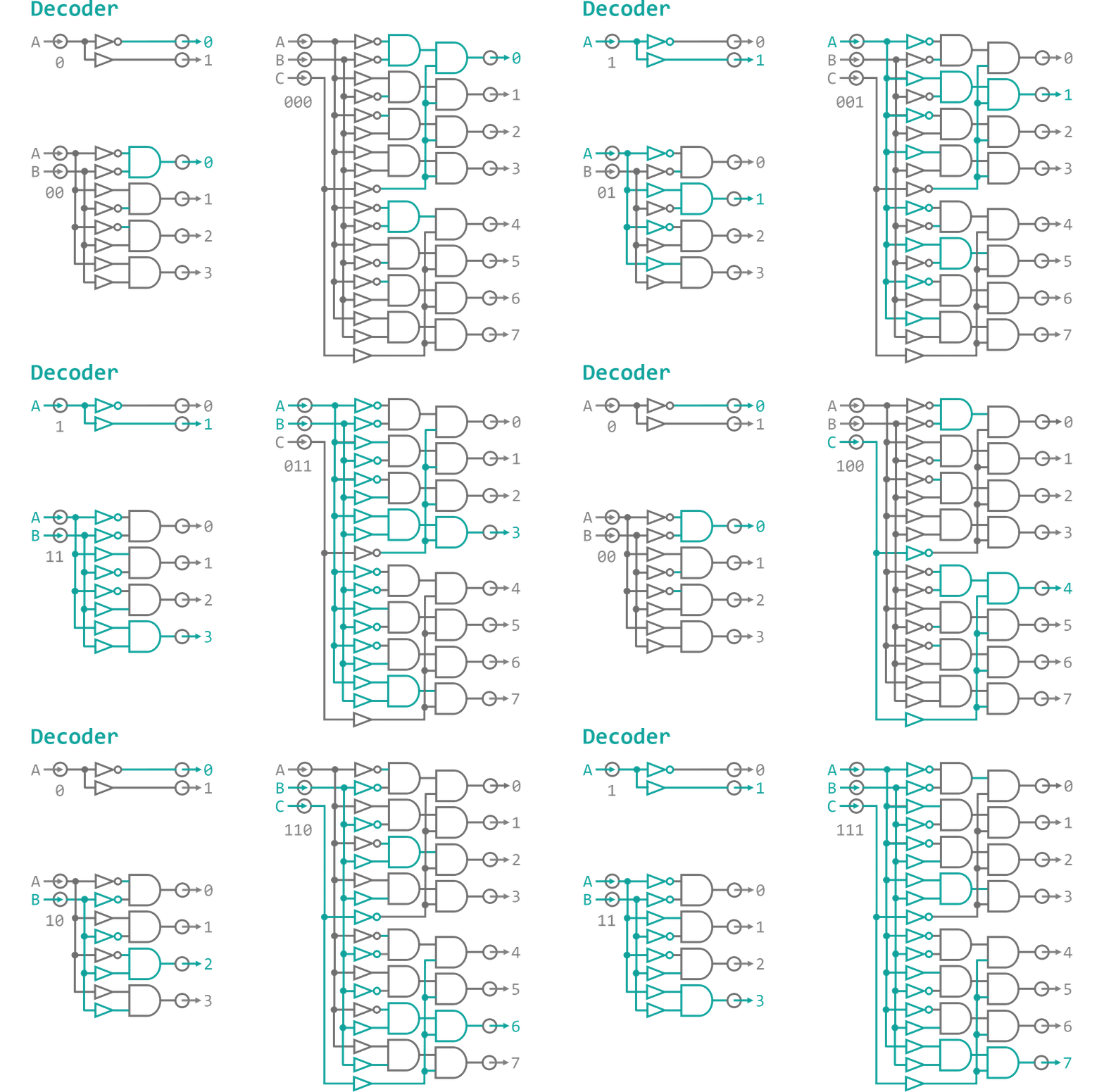
As you can see every output is made up from a unique combinations of buffers and NOT gates that are fed into ANDs. Basically, when you want to address the 5th output (thats 0110 in binary) you place a buffer where you expect the input Bit to be high and a NOT gate where it will be low. That way, all resulting inputs to the AND gates for a specific output are high when the appropriate address is dialed (0110 → NOT, BUFFER, BUFFER, NOT → 1111). Every instruction will have a BUS junction consisting of a address decoder that dis-/enables the clock phase I and III inputs to the component, thereby, effectively switching the instructions on and off as needed. Additionally if you want to input something into the BUS you need to make sure the input does not collide with data that is already present on the BUS. Since data will only flow one way through our system and the clock cycles make sure that with have plenty of time before things are shuffled around, this should not be an issue here. However, for completeness sake - and because Logisim constantly complains otherwise - I have included multi-Bit OR gates everywhere where there is the need to merge data onto the BUS. A logic gate that is applied to a multi-Bit connection just applies the operation to all individual Bit lines in parallel. Using this notation instead of copying thousands of separate gates that take in Bit 0 of lines A and combine it with Bit 0 of line B, and so on just makes it a little more tidy. Using this knowledge I finished the Arithmetic-Logic-Unit as can be seen in Figure 2.
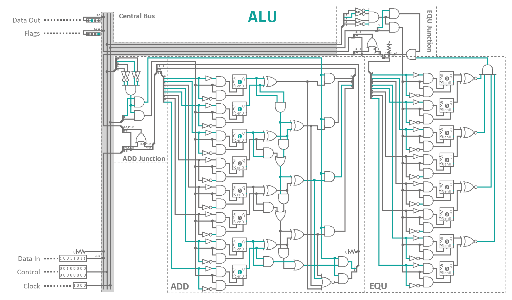

Besides the aforementioned connection to a main BUS via junctions, I took the liberty of adding the second ALU instruction called EQU. It is the equality compare operation which takes in two 4‑Bit operands and compares them for equality Bit-wise using XNOR gates. The four results are merged into a single output via a AND gate and are fed into the third Bit of the flag data line. Hence, this flag hereinafter shall be known as EF (equality flag). The remaining forth flag Bit is reserved, i.e. I added it in case we required another status flag for future applications. Overall this yield a 12‑Bit Data Bus carrying 4 Flag Bits, 2 × 4 Bits for data input and 4 Bits for data output. Next are 4 Bits representing the four clock phases. Yes, there exists a fourth phase, called pre-phase, where the next piece of code is read in and everything is setup accordingly, before we light off the instruction itself (commonly called fetch). More about this in the next part. And last but not least, there is a 16‑Bit control bundle which, apart from the four instruction address Bits, looks awfully empty at the moment. Most of the remaining Bits (9 to be more precise) will control the short-term memory of the processor, called general purpose registers. Figure 3 shows the circuit diagram for one of those 4‑Bit memory cells.
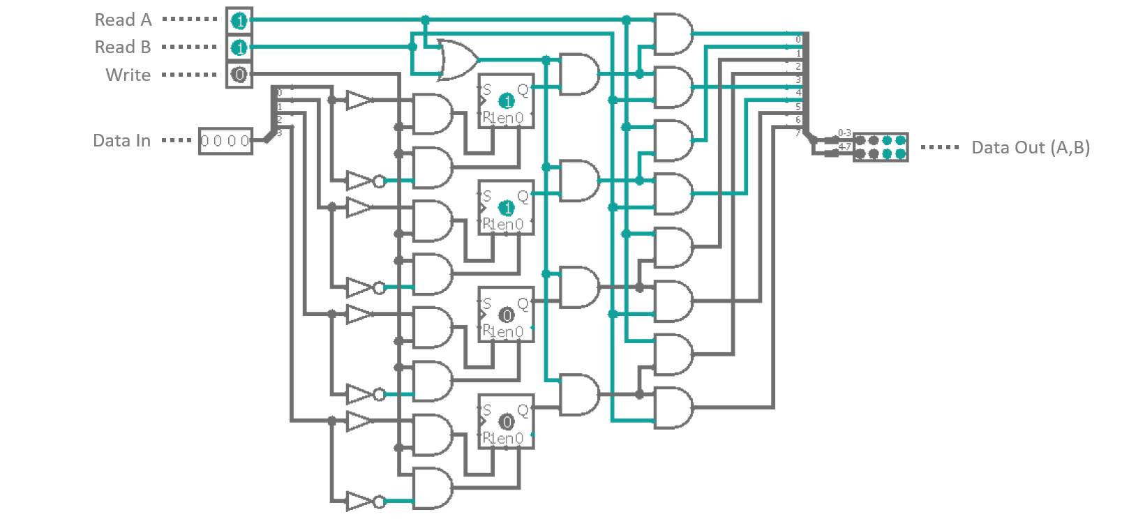
This should look suspiciously familiar to you as this is pretty much what we have used as input cache for our ALU instructions. The only difference is, that the registers have two separate output lines instead of one. Three different control inputs steer the functionality of the component. 'Write' will be synchronous with clock phase III and will transfer whatever is currently present in the 'output' part of the data BUS into the register. 'Read A' and 'Read B' will push the content of the register onto the corresponding 'inputs' of the data BUS, in sync with clock phase I. So, in theory you could simultaneously enable all three operation modes of a single register (separated only by the corresponding clock cycles) together with the e.g. the ADD instruction. Clock phase I would set data input A and B of the BUS to the value stored in the register. At the same time the input cache of ADD was activated, all in all copying the value to both operands of the instruction. With clock phase III the result was released into the data output which in return gets fed back into the register... a nice way of doubling the register's value with every repitition of the steps.
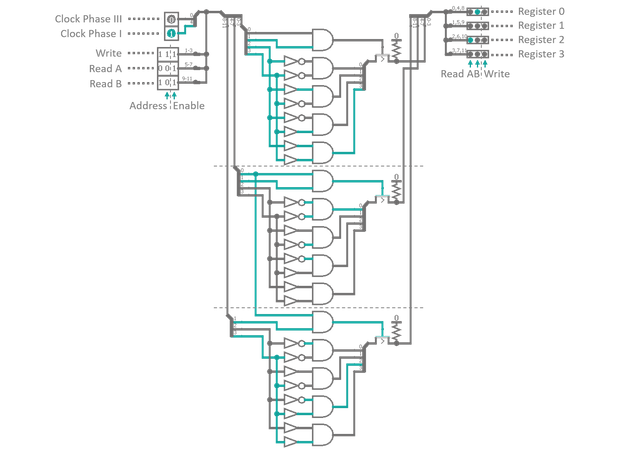
Altogether, our processor will be given four general purpose registers. That is oddly generous for such a puny, little critter. However, I do not intend of adding any other form of writable memory to the system, so these four registers will be all the space we have to shuffle around results and operands. May this justify the utter debauchery. Wait a second, 4 × 3 required control inputs results in 12 input connections in total. How do we manage to serve 12 inputs with only 9 Bits on the control BUS? Again the answer to this question is decoders. Figure 4 displays the register controller in all its beauty. 'In' go the clock phases I and III as well as three 3‑Bit control inputs. The first Bit of each is a simple 'enable' switch for the feature itself. The other two Bits are for addressing the target register for the selected operation mode. The three addresses are fed into a decoder each, which outputs a high signal on the corresponding of its four outputs. When both, the enable Bit and the respective clock input, are high at the same time a 4‑Bit transistor gate is opened transferring the decoder result to the registers. The gating is necessary as the decoder will always output something, so, in order to disable a feature entirely we need to explicitly suppress the output. Via a resistor we pull all controls to GND by default. When a gate opens, one of the four output lines is overwritten by the decoder result, activating the selected registers according operation mode. In the end, apart from the decoding step, it is just a little rerouting of connections.
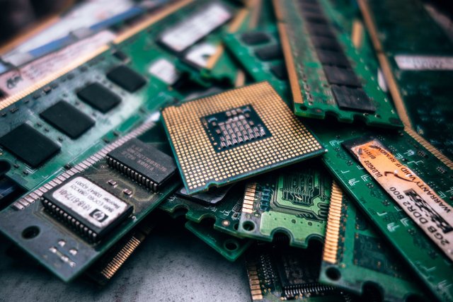
Deeeeeeeeeeetouuuuuur. I have been very dutiful this time, giving you a big, solid chunk of information without a single deviation from track... I have earned myself a digression. Let's begin our delve into the world of science by asking: "Is it necessary for our processor to have registers?". The answer clearly is: NO. A processor just needs some way of handling operands, i.e. loading and storing variables and results. Think of it like a workbench in a shop. You have your tools which represent the instructions and your building material substituting data. You could argue that it might be possible to build e.g. a diesel motor by throwing all the parts way high up into the air and then process and assemble everything before it hits the ground. However, even though it will definitely look mighty impressive, this obviously is by far not the easiest way of accomplishing your task. It would be much more convenient to set aside those components you are currently not working on or lay things away whilest you are changing tools. The same applies to a processor: You need space to work within. This space is called memory and it occurs in many different flavours: Registers are without a doubt very handy as they are usually connected to the main BUS directly. Therefore, data transfer between instructions and registers in first approximation happens instantly. It is, however, just not feasible to slam 32 GB of registers into a CPU, as this - upon other reasons - would make your processor obscenely ginormous (and therefore impossible to route onto a single piece of silicon). Instead, dedicated additional memory is added via a common interface from outside. This external memory is usually referred to as dynamic random access memory DRAM and comes in compact sticks (see figure 5 for an artistic impression). Compared to registers this memory usually is much slower (you have to push the data through the interface bottleneck) making memory transaction expensive in regards to calculation time. Therefore, modern CPU contain a little bit of extra storage beyond their registers, called cache. It is used to load chunks of data from main memory into the CPU in anticipation of a later usage. Imagine you are processing a file block-wise. Instead of reading every individual block, processing it and than waiting for the next one, your CPU will buffer the next couple hundred of blocks into its cache, in order to make the following block operations happen much faster. If the additionally cached information is not needed, nothing is lost... at least from a timing perspective. The CPU does not know about file borders or implemented access restrictions. If you read something the processor will just cache everything in its immediate vicinity. In theory you could gain access to protected areas of memory by reading blocks that lie adjacent to them and then scanning the CPU's cache. With a little luck, the processor greedily stuffed forbidden memory regions into its temporary storage together with the originally requested data. Oops, we have just discovered the Spectre security vulnerability that recently unsettled the IT community [1].
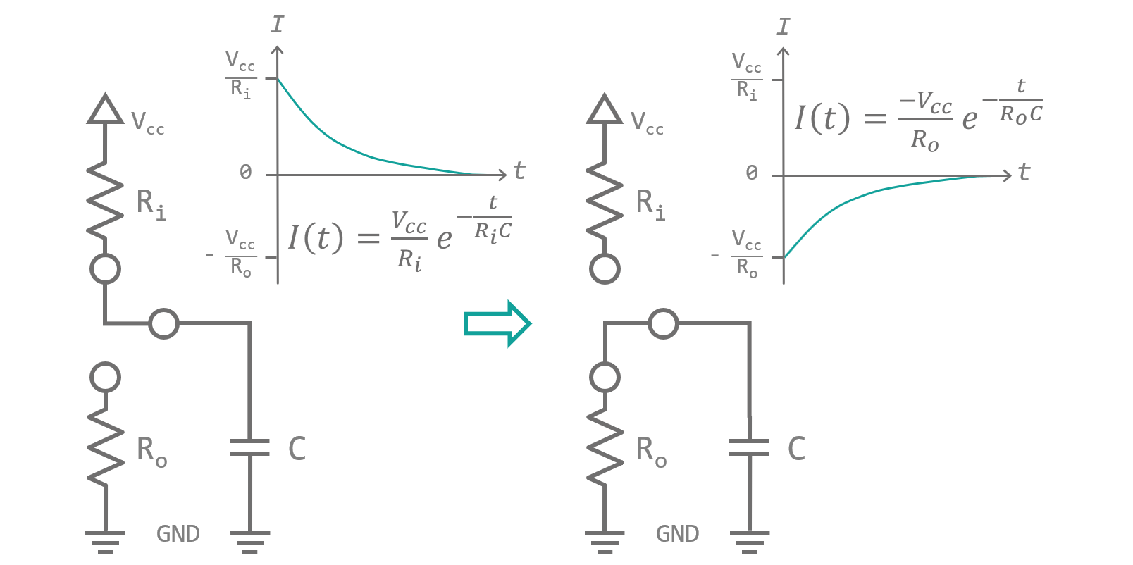
Wow, I managed to get sidetracked from my sidetrack. *Excessive throat clearing* RAM, cache, and registers are so called volatile memories, i.e., they only store information for a short period of time. At the latest, when you turn the device off, volatile memory rapidly suffers from amnesia. How exactly do these types of memory work? They rely on a physical phenomenon called electrical capacity. Think of it as the capability of storing electrical charges. Every time, two conducting surfaces get in close proximity of each other, they form what is called a capacitor. Even though, no currents can directly pass from one surface to the other, when you apply a voltage across the gap, a current flows (see figure 6). Voltage is similar to pressure in Newtonian mechanics. It pushes electrons from the negative source into the the connected surface, leading to the built up of negative charges. If the overall charge becomes strong enough, its static electrical field influences the electrons in the opposite surface, pushing them away (directed by Coulomb forces). A charge with opposite sign but equal amount is formed (called a mirror charge). No electrons crossed the gap, nevertheless, if you watch what happens at either of the sides, you will see electrons frolicking their way towards and away from the gap... a virtual current is flowing, called displacement current. This current will decrease exponentially over time, even if the electron source is providing a constant voltage. The charges in the capacitor evoke an electrical field opposite to the one created by the voltage source. At some point an equilibrium is reached and no more electrons can be forced into or out of the capacitor. Quite comparable to compressing a metal spring, by building up this field inside the capacitor, energy is stored. When the gap is not empty but filled with a so called dielectric, its capacity can be further increased. A dielectric is made up of atoms or molecules that are built in an asymmetrical manner. When they are superposed with an electrical field they will align against the field like little compass needles. The energy required to turn all of them in the direction of the field lines adds to the amount of energy stored by the capacitor. Finally, when the capacitor is disconnected from the voltage source it keeps its charge until a resistor is shunted across it. In that case the stored energy forces the electrons through the resistor balancing the charges between the two contacts. Again a current flows that slowly decays as the electrical field in the capacitor collapses. A DRAM ist built from capacitors and transistors. At least in theory, writing an individual Bit is as simple as charging the capacitor. Storing the information means disconnecting it and reading accounts as discharging it. Of course, the devil lies in the detail. You do not necessarily want to discharge the capacity when reading it, as this will destroy the stored information. Also, small leakage currents will drain the capacitor no matter what you do, so you have to refresh all Bits in regular cycles.
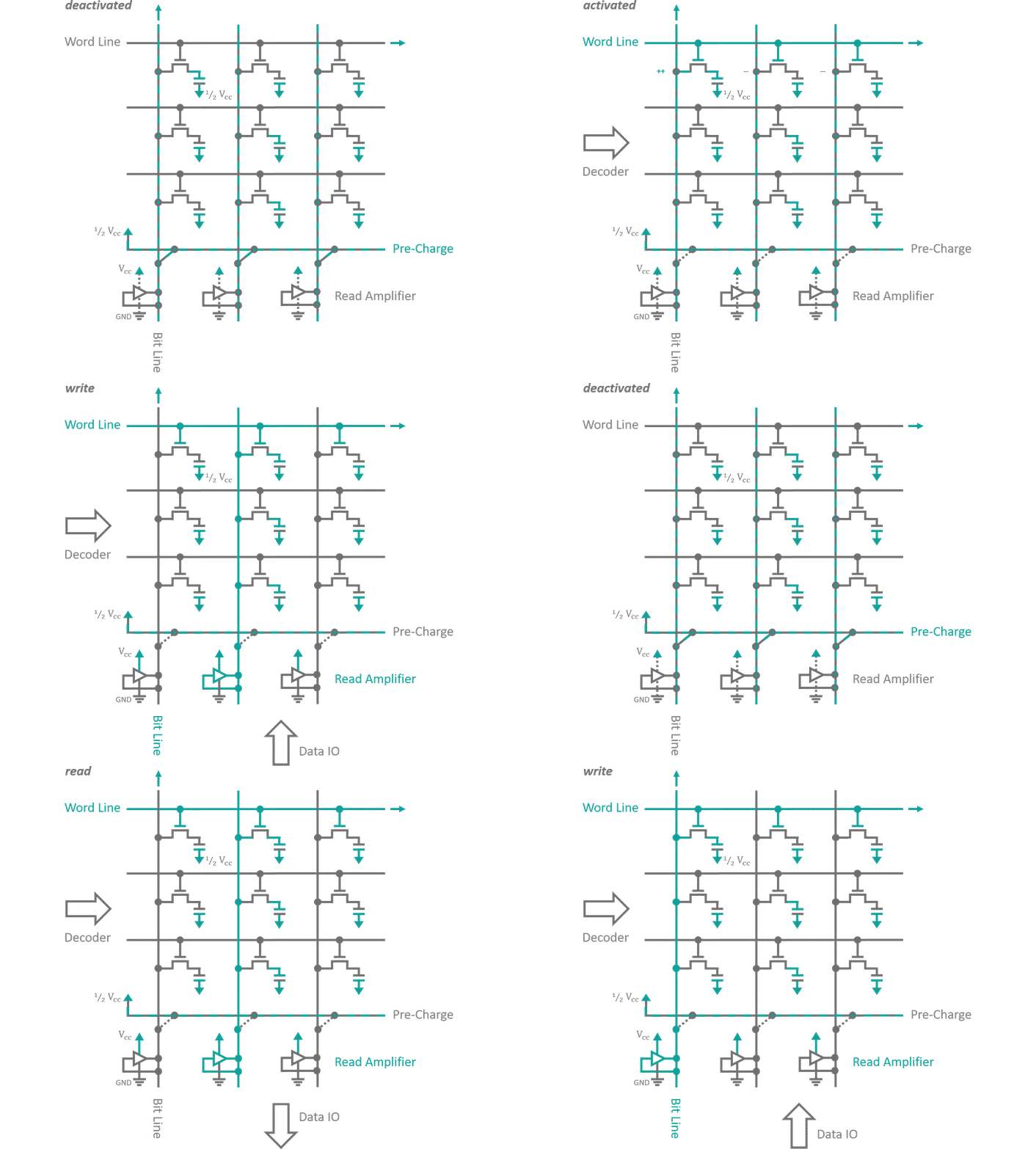
Without going into too much detail, DRAM memory is made from a grid like structure of transistors as can be seen in figure 7. Every transistor feeds into a capacitor for single Bit storage. Each row of cells has its transistor gates connected to a common selector line (Word line). Columns of cells have their source connection joined into individual Bit lines. While a memory region is deactivated, its Bit lines are charged with a voltage that resembles half of the 'High' signal voltage. When you want to read a specific row of Bits, first you need to disconnect the charging voltage, than you active the the corresponding Word line. As the transistors become conductive, a charge exchange between the Bit line and the storage capacitors occurs until both carry an averaged charge. Depending on whether the capacitor was initially charged, i.e. the Bit was set or not, this average will ris above or fall below the Bit line's pre-charge. A read amplifier connected to the Bit lines is activated, which discriminates the small charge differences into logic states and sets the Bit lines to 'High' or 'Low' potential accordingly. This recharges the storage capacitors to full potential and allows pushing the read out bits onto the outgoing data BUS. Writing is as simple as pushing the input data into the read amplifiers, effectively overwriting their current states. The new states will either charge or discharge the connected storage capacitors accordingly. All thats left to do in either case, is to deactivate the transistors by removing the signal of the Word line, disabling the read amplifiers and reconnecting the Bit lines to the pre-charge voltage. This happens within a couple nanoseconds (which is considered rather slow) but can be engineered to reach insane memory densities. Once again, this technology has it's flaws. When multiple very small capacities are crammed into as little space as possible it is almost impossible to properly shield them against each other. By accessing a memory region in very high frequencies you are forcing the RAM to charge and discharge the storage capacitors of the desired data row. Their electrical dipole moment will couple to all surrounding capacities. A recently discovered vulnerability known as Rowhammer exploits this by quickly alternating access between two memory regions sandwiching a deactivated third one. It has been proven [2] that the coupling between capacitors is strong enough to enforce the flipping of bits in the deactivated memory region. As you can imagine, this opens up for countless attack scenarios on critical memory regions. One more note on volatile memory in general: In my processor simulation I used NOR gate RS-latches for the registers (Gate based RAM is referred too as static random access memory SRAM). No one in their right minds would do that in real life applications, nowadays. If toggling single transistors, specifically engineered for memory purposes, are considered 'slow', you can calculate for yourselves how long it takes a Bit to traverse a d-latch consisting of something closer to 10 transistors. This design decision was forced upon me by Logisim, which does not allow for the simulation of dynamic (using capacitors instead of gates) memory cells. It does not matter too much though, since Logisim actually does not include run times what so ever in the simulation steps... everything happens simultaneously anyways. Just keep that in mind when you are actually trying to pirate my design to etch and mass produce these advanced '4‑Bit, 8 instruction' Behemoths of digital engineering.
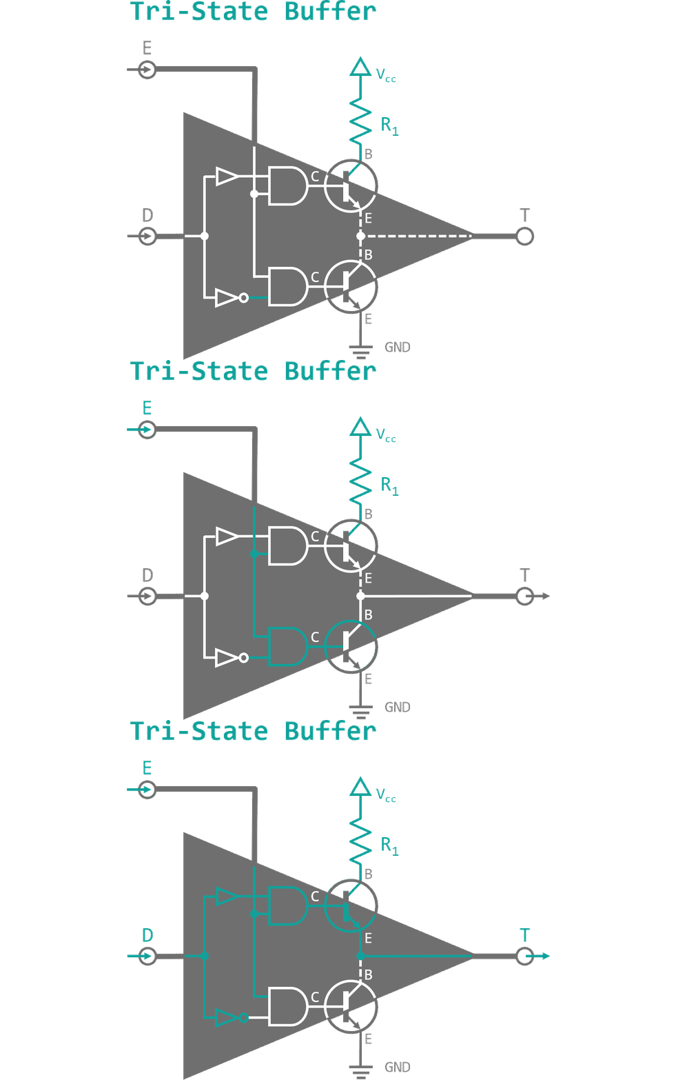
Last but not least, I want to introduce you to another interesting application using capacitors. Figure 8 shows a component called tri-state buffer. Different from all logic components, I have presented to you so far, it has a third logic state (hence its name) besides 'High' and 'Low'. When the enable pin (E) is deactivated both output transistor are in blocking mode. The output connection T then is neither connected to GND nor Vcc and therefore floats on a high impedance (connected to "air") level. When E receives a high signal, depending on the data pin (D), either of the output transistors will be activated, connecting the output to GND or Vcc accordingly. Since a connection is a conductive surface it will always resemble a capacitor in reference to GND level. This is called parasitic capacity and it is usually an unwanted feature. By connecting two or more tri-state buffers in series though, we can take advantage of this phenomenon. When the enable pins of our tri-state chain are connected through NOT gates to each other, every other buffer will be enabled. See figure 9 for a schematic.

When a signal is present, while the first tri-state is active, the capacity between this buffer and its deactivated neighbor will be charged. As we toggle our control input, connection is lost to the input. The capacity discharges into the data input of the next tri-state buffer, which is now enabled and transfers charge to the next inter-buffer capacity. With every control signal flip, the charge on the parasitic capacity between buffers moves to the next cell. This arrangement is called a dynamic master slave Flip-Flop and it allows us to carry a Bit down a bucket chain, in sync with an external trigger. This external trigger could for example be a resonating quartz. A piece of silicon-oxide mineral (quartz) that is stuffed into a capacitor. When an electric field is applied to the quartz it will slightly deform, storing energy in its mechanical tension. As the field vanishes the quartz relaxes and converts its internal energy back into an electrical field (piezo electric effect. This signal can be amplified an fed back into the quartz provoking an oscillation between electrical and mechanical energy. The resonance frequency range of a quartz oscillator is very narrow, so they provide a signal with high precision. On top of that, the venter frequency is almost independent of environmental influences like temperature jitter. Both, its stability and its precision, make quartz oscillators perfect for usage as external clock drivers in digital applications. The clock, that will be used for our processor is depicted in figure 10.
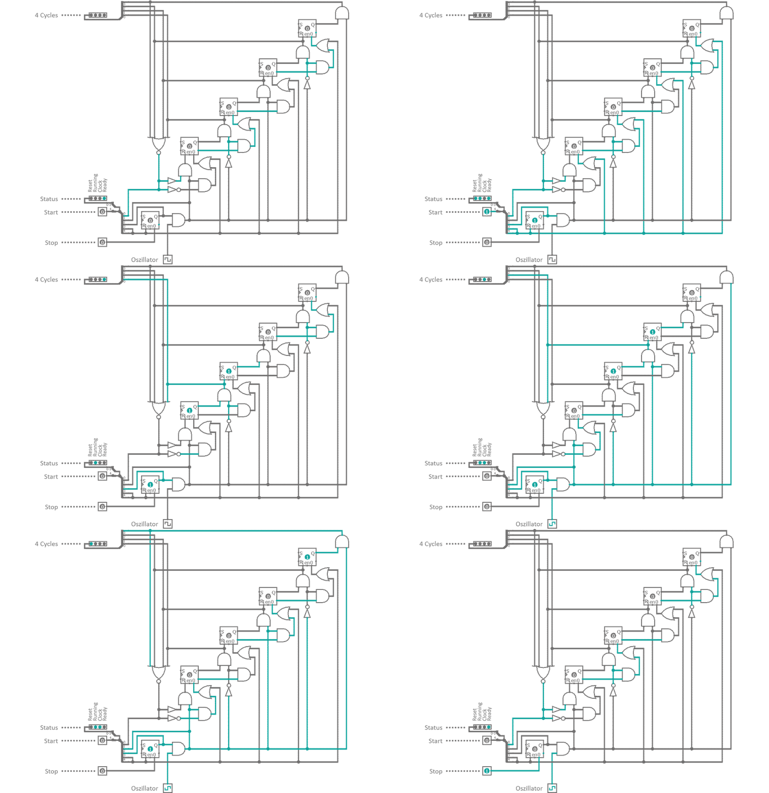
It consists of a 4 cell dynamic master-slave flip-flop chain, a feedback line and some controls as well as the external oscillator. When a 'Start' signal is received, a RS-latch is toggled, which enables the clock and a reset line is enabled. Reset removes all high Bits from the flip-flop bucket chain. As soon as 'Start' is released (and reset deactivates) the first clock cycle begins. All bucket chain outputs are connected to a 4 input NOR gate. As reset deleted all Bits, the NOR gate does not see a high signal on any of its pins and outputs a high Bit, which is used to bootstrap the charge traversing the flip-flops. With every external oscillator toggle, the charge enables all four clock phase outputs one after another. Finally, when the charge is emitted at the last flip-flop, the NOR gat feedback kicks back in and invokes a now cycle. A 'Stop' signal from the controller resets the status RS-latch and the oscillator input is suppressed. The clock halts and is ready for a restart.
We have talked a lot about volatile memory this time. But what about non-volatile memory? This question as well as, how we will program our processor, will be answered in the next part. Stay tuned.
[1] Spectre Paper (pdf)
[2] Rowhammer Paper (pdf)