Exploring and manipulating the behavior of polar vortices in material may lead to new technology for faster data transfer and storage from Argonne National Lab Press Release on emergent phenomena. New Type of Matter? Will Photonic chips bring change?
2018 from Seeker
From this video and article titled
Photonic Chips will change computing forever. . .if we can get it right!
Hear him say, "even though scientists have been trying since the 60's, an optical transistor that can replace an electrical one has never materialized.
Like trying to build a photonic chip that mimics the way a human brain performs calculations.
Scientists at MIT have built a chip that uses beams of light sent through a channel of silicon to mimic a neural network.
The beams split and combine and travel at different speeds as the silicon is heated and cooled.
They've applied this tech to train a neural network to understand vowel sounds with some success.
They think they can improve their results dramatically by making a purpose built system instead of the jury-rigged proof of concept
Reported by Nonur in 2019
Thinnest optical waveguide channels light within just three layers of atoms
August 13, 2019 by nonur
Engineers on the College of California San Diego have developed the thinnest optical machine on the planet — a waveguide that’s three layers of atoms skinny.
The work is a proof of idea for cutting down optical units to sizes which are orders of magnitude smaller than in the present day’s units. It may result in the event of upper density, larger capability photonic chips. Researchers revealed their findings Aug. 12 in Nature Nanotechnology.
“Basically, we show the last word restrict for a way skinny an optical waveguide could be constructed,” stated senior writer Ertugrul Cubukcu, a professor of nanoengineering and electrical engineering at UC San Diego.
The brand new waveguide measures about six angstroms skinny — that’s greater than 10,000 occasions thinner than a typical optical fiber and about 500 occasions thinner than on-chip optical waveguides in built-in photonic circuits.
The waveguide consists of a tungsten disulfide monolayer (made up of 1 layer of tungsten atoms sandwiched between two layers of sulfur atoms) suspended on a silicon body. The monolayer can also be patterned with an array of nanosized holes forming a photonic crystal.
“This additionally makes it the thinnest optical resonator for seen gentle ever to be demonstrated experimentally,” stated first writer Xingwang Zhang, who labored on this undertaking as a postdoctoral researcher in Cubukcu’s lab at UC San Diego. “This technique doesn’t solely resonantly improve the light-matter interplay, but additionally serves as a second-order grating coupler to couple the sunshine into the optical waveguide.”
Researchers used superior micro- and nanofabrication methods to create the waveguide. Creating the construction was significantly difficult, stated Chawina De-Eknamkul, a nanoengineering PhD pupil at UC San Diego and a co-author of the research. “The fabric is atomically skinny, so we needed to devise a course of to droop it on a silicon body and sample it exactly with out breaking it,” she stated.
The method begins with a skinny silicon nitride membrane supported by a silicon body. That is the substrate upon which the waveguide is constructed. An array of nanosized holes is patterned into the membrane to create a template. Subsequent, a monolayer of tungsten disulfide crystal is stamped onto the membrane. Ions are then despatched by way of the membrane to etch the identical sample of holes into the crystal. Within the final step, the silicon nitride membrane is gently etched away, leaving the crystal suspended on the silicon body. The result’s an optical waveguide by which the core consists of a monolayer tungsten disulfide photonic crystal surrounded by a cloth (air) with a decrease refractive index.
Transferring ahead, the staff will proceed to discover the elemental properties and physics pertaining to the waveguide.
By September of 2019 according to Opli
In an article titled,
Creating Different Kinds of Light with Manipulable Quantum Properties
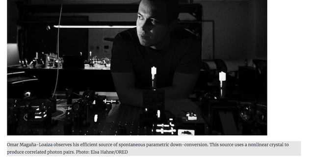
Omar Magaña-Loaiza, assistant professor in the LSU Department of Physics & Astronomy, and his team of researchers describe a noteworthy step forward in the quantum manipulation and control of light, which has far-reaching quantum technology applications in imaging, simulation, metrology, computation, communication, and cryptography, among other areas. The paper, titled “Multiphoton quantum-state engineering using conditional measurements,”
While physicists can so far control the quantum properties of single photons and pairs of photons, leading to powerful applications through entanglement and “heralding” (wherein knowledge of one photon gives relatively certain knowledge about another, not-yet-detected photon), Magaña-Loaiza’s team successfully demonstrated a method to generate groups of photons with these same powerful properties—known as multiphoton states. By subtracting out some photons, Magaña-Loaiza said, “we can reshape the form of the wavepacket and artificially increase the number of photons in it.” Moreover, whereas previous scientists produced multiphoton states using multiple sources, Magaña-Loaiza’s team managed to build a single source to produce multiphoton packets that share similarities with entangled lasers: a major technological achievement.
And just a month prior in August of 2020 you have. ..
from San Diego Biotech Networks
Biologists Pioneer First Method to Decode Gene Expression

Interesting as this organization also reported on this. . .

Tech Crunch in 2021
AI is fundamental to many products and services today, but its hunger for data and computing cycles is bottomless. Lightmatter plans to leapfrog Moore’s law with its ultra-fast photonic chips specialized for AI work, and with a new $80 million round, the company is poised to take its light-powered computing to market.
Lightmatter’s chips perform in a flash — literally — certain complex calculations fundamental to machine learning. Instead of using charge, logic gates and transistors to record and manipulate data, the chips use photonic circuits that perform the calculations by manipulating the path of light. It’s been possible for years, but until recently getting it to work at scale, and for a practical, indeed a highly valuable purpose, has not.
It wasn’t entirely clear in 2018 when Lightmatter was getting off the ground whether this tech would be something they could sell to replace more traditional compute clusters like the thousands of custom units companies like Google and Amazon use to train their AIs.
“We knew in principle the tech should be great, but there were a lot of details we needed to figure out,” CEO and co-founder Nick Harris told TechCrunch in an interview. “Lots of hard theoretical computer science and chip design challenges we needed to overcome… and COVID was a beast.”
“In general what we’re doing is pretty crazy,” he admitted. “We’re building computers from nothing. We design the chip, the chip package, the card the chip package sits on, the system the cards go in, and the software that runs on it…. we’ve had to build a company that straddles all this expertise.”
Where a few years ago Lightmatter’s product was more of a well-informed twinkle in the eye, now it has taken a more solid form in the Envise, which they call a “general-purpose photonic AI accelerator.” It’s a server unit designed to fit into normal data center racks but equipped with multiple photonic computing units, which can perform neural network inference processes at mind-boggling speeds. (It’s limited to certain types of calculations, namely linear algebra for now, and not complex logic, but this type of math happens to be a major component of machine learning processes.)
It’s Lightmatter’s initial plan to test these units with its most likely customers by the end of 2021, refining it and bringing it up to production levels so it can be sold widely. But Harris emphasized this was essentially the Model T of their new approach.
“If we’re right, we just invented the next transistor,” he said, and for the purposes of large-scale computing, the claim is not without merit. You’re not going to have a miniature photonic computer in your hand any time soon, but in data centers, where as much as 10% of the world’s power is predicted to go by 2030, “they really have unlimited appetite.”
There are two main ways by which Lightmatter plans to improve the capabilities of its photonic computers. The first, and most insane-sounding, is processing in different colors.
It’s not so wild when you think about how these computers actually work. Transistors, which have been at the heart of computing for decades, use electricity to perform logic operations, opening and closing gates and so on. At a macro scale you can have different frequencies of electricity that can be manipulated like waveforms, but at this smaller scale it doesn’t work like that. You just have one form of currency, electrons, and gates are either open or closed.
In Lightmatter’s devices, however, light passes through waveguides that perform the calculations as it goes, simplifying (in some ways) and speeding up the process. And light, as we all learned in science class, comes in a variety of wavelengths — all of which can be used independently and simultaneously on the same hardware.
The same optical magic that lets a signal sent from a blue laser be processed at the speed of light works for a red or a green laser with minimal modification. And if the light waves don’t interfere with one another, they can travel through the same optical components at the same time without losing any coherence.
That means that if a Lightmatter chip can do, say, a million calculations a second using a red laser source, adding another color doubles that to two million, adding another makes three — with very little in the way of modification needed. The chief obstacle is getting lasers that are up to the task, Harris said. Being able to take roughly the same hardware and near-instantly double, triple or 20x the performance makes for a nice roadmap.
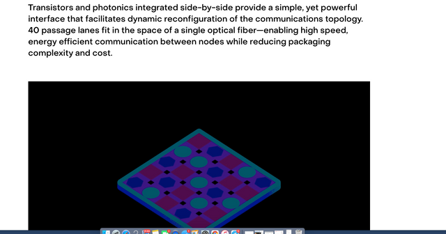
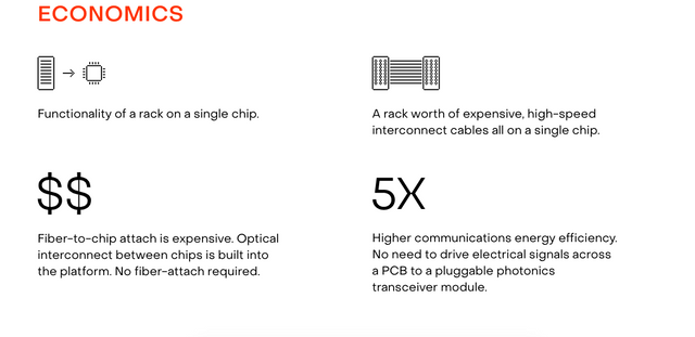
It also leads to the second challenge the company is working on clearing away, namely interconnect. Any supercomputer is composed of many small individual computers, thousands and thousands of them, working in perfect synchrony. In order for them to do so, they need to communicate constantly to make sure each core knows what other cores are doing, and otherwise coordinate the immensely complex computing problems supercomputing is designed to take on.
“One of the things we’ve learned along the way is, how do you get these chips to talk to each other when they get to the point where they’re so fast that they’re just sitting there waiting most of the time?” said Harris. The Lightmatter chips are doing work so quickly that they can’t rely on traditional computing cores to coordinate between them.
A photonic problem, it seems, requires a photonic solution: a wafer-scale interconnect board that uses waveguides instead of fiber optics to transfer data between the different cores. Fiber connections aren’t exactly slow, of course, but they aren’t infinitely fast, and the fibers themselves are actually fairly bulky at the scales chips are designed, limiting the number of channels you can have between cores.
“We built the optics, the waveguides, into the chip itself; we can fit 40 waveguides into the space of a single optical fiber,” said Harris. “That means you have way more lanes operating in parallel — it gets you to absurdly high interconnect speeds.”


Find specs here,
https://lightmatter.co/products/passage/
Also in August of 2019
As reported by Science Bulletin
Dyes and viruses create new composite material for photo-oxidation reactions
August 12, 2019
A recent study, published in Advanced Materials, shows that native viruses can be employed as a scaffold to immobilise photoactive molecules to potentially oxidise organic pollutants present in wastewater, under visible light irradiation
A research team from Aalto University has developed a novel strategy to create virus-based materials for catalysis. The project, which is framed within the Horizon 2020 Marie Skłodowska-Curie actions, aims to pave the way towards the application of optically active biohybrid materials—a combination of biomolecules and synthetic moieties—in topics ranging from nanomedicine to green organic synthesis or environmental sciences.
“Our first challenge was to select the right photosensitizer,” says Eduardo Anaya, postdoctoral researcher at Aalto University, “We decided to employ phthalocyanines, a synthetic derivative of hematoporphyrin (the dye responsible for the colour of blood), due to their outstanding properties as a reactive oxygen species generator. However, the use of this kind of dyes in aqueous media presents several challenges that affect their performance. Therefore, careful design was necessary to maintain their properties`.
In collaboration with Professor Tomas Torres’ research group from the Universidad Autonoma de Madrid, a new phthalocyanine derivative was synthesised, resulting in a molecule with resilient properties in different ionic strength media. The design ensured the photoactivity of the dye even in an aqueous environment.
“One of the focuses of our research group lies in the design of new protein assemblies and their potential application as new materials’ adds Professor Mauri Kostiainen, leader of the Biohybrid Materials group. “Our approach is based on supramolecular interactions, such as electrostatic binding so, in this project, we decided to combine the positively charged dye with a negatively charged tobacco mosaic virus (a 300 nm long rod-like virus), resulting in a photoactive fibrous material. This approach led to highly ordered threads, which were thoroughly characterised by X-ray scattering and several microscopy techniques in the Nanomicroscopy Center at Aalto,” Kostiainen says.
In addition to the structural characterisation, Anaya points out that the most crucial feature is that the dye remains active despite being immobilised in the fibres. ´We can fix the reaction site in solid support and pass the solution we want to react through it, being visible light the only “fuel” we use for it to happen. This allows us to create a continuous flow set-up that enable the scaling up of the oxidation process,” he concludes.
The research team designed a proof-of-concept device where immobilising the fibres within a glass capillary; an incoming flow was oxidised in several cycles. The resilience of the fibres was assessed, concluding that both their structural stability and photoactivity remain constant over time. One additional advantage is that, once the oxidation process is completed, a light pulse can disassemble the fibres, making them easy to dispose of. The reported approach represents the first step towards the use of biohybrids in continuous flow reactions, which represent an environmentally friendly approach to this type of industrial process.
Key phrasing. . .Hybrid and "environmentally friendly"
By June 1, 2021
At Endhoven University of Technology
Netherlands tames the light in photonic chips
Photonic chips, powered by light rather than electricity, are the future. They will pave the way for self-driving vehicles, innovations in healthcare, and, of course, energy-efficient data and telecommunications.
The possibilities of our current electronic chip technology are slowly but surely reaching their limits due to resistance, which is released in the form of heat as electrons travel through the copper conduits between transistors in chips. That resistance weakens the signal as it passes through the material.
Sylwester Latkowski, TU/e researcher and the brand-new scientific director of the Center: "This R&D center will build a bridge to really get photonic chips to the market. In fact, we experience a gap when it comes to maturing the technology. As researchers, we work up to an advanced prototype, but the industry lacks the resources to move forward with that," Latkowski explains.
He continues: "Our role model is imec, the R&D hub for nano and digital technologies for semiconductor electronics industry. With them you really see how much value there is of having a large center for research and development in the chain. And that such an overarching center can perfectly well co-exist alongside the established institutes, start-ups, companies, large industries and universities."
. ..we also differ from academia. We're not targeting papers or mentoring PhD students. We are purely focused on what the industry is looking for, what the next generation products and applications need and at what moment which product is wanted," he explains.
That there is a market for cost-effective integrated photonic chips is apparent when we look at self-driving cars. Photonic components are already in use for the cameras and LIDAR modules that provide full surveillance of the surrounding and allow the vehicle to accelerate and brake automatically.
But one LIDAR sensor of an autonomous Google car, for example, can cost as much as 60.000 dollars. An autonomous car needs at least 6 of such sensors to be able to view the surroundings with sufficient extent of detail and not make any mistakes.
Latkowski: “The car industry has calculated that the photonic components should cost a maximum of 50 dollars to be a cost-effective solution for the car market. Integrated photonics can then be a game-changer. It brings many advantages over discrete component-based photonic systems, in terms of size, stability, performance, reliability, and cost.”
Note from 2016 in Nature
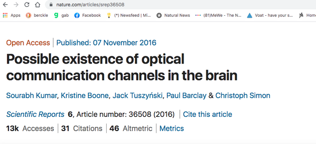
https://www.nature.com/articles/srep36508
https://www.nature.com/articles/s41586-018-0028-z
Characteristics of Optical Channel for Underwater Optical
Wireless Communication System
https://www.iosrjournals.org/iosr-jeee/Papers/Vol10-issue2/Version-1/A010210109.pdf
Interesting!
ECEN689: Special Topics in Optical
Interconnects Circuits and Systems
Spring 2020
Sam Palermo
Analog & Mixed-Signal Center
Texas A&M University
https://people.engr.tamu.edu/spalermo/ecen689_oi/lecture2_ee689_optical_channels.pdf
According to Phys.org

Unlike ordinary transistors, which can be either "0" (off) or "1" (on), qubits can be both "0" and "1" at the same time. The ability of individual qubits to occupy these so-called superposition states, where they are in multiple states simultaneously, underlies the great potential of quantum computers. Just like ordinary computers, however, quantum computers need a way to transfer quantum information between distant qubits—and that presents a major experimental challenge.
In a series of papers published in Nature Communications, researchers at the University of Rochester, including John Nichol, an assistant professor of physics and astronomy, and graduate students Yadav Kandel and Haifeng Qiao, the lead authors of the papers, report major strides in enhancing quantum computing by improving the transfer of information between electrons in quantum systems.
In one paper, the researchers demonstrated a route of transferring information between qubits, called adiabatic quantum state transfer (AQT), for the first time with electron-spin qubits. Unlike most methods of transferring information between qubits, which rely on carefully tuned electric or magnetic-field pulses, AQT isn't as affected by pulse errors and noise.
To envision how AQT works, imagine you are driving your car and want to park it. If you don't hit your brakes at the proper time, the car won't be where you want it, with potential negative consequences. In this sense, the control pulses—the gas and brake pedals—to the car must be tuned carefully. AQT is different in that it doesn't really matter how long you press the pedals or how hard you press them: the car will always end up in the right spot. As a result, AQT has the potential to improve the transfer of information between qubits, which is essential for quantum networking and error correction.
The researchers demonstrated AQT's effectiveness by exploiting entanglement—one of the basic concepts of quantum physics in which the properties of one particle affect the properties of another, even when the particles are separated by a large distance. The researchers were able to use AQT to transfer one electron's quantum spin state across a chain of four electrons in semiconductor quantum dots—tiny, nanoscale semiconductors with remarkable properties. This is the longest chain over which a spin state has ever been transferred, tying the record set by the researchers in a previous Nature paper.
Exploiting a strange state of matter
In a second paper, the researchers demonstrated another technique of transferring information between qubits, using an exotic state of matter called time crystals. A time crystal is a strange state of matter in which interactions between the particles that make up the crystal can stabilize oscillations of the system in time indefinitely. Imagine a clock that keeps ticking forever; the pendulum of the clock oscillates in time, much like the oscillating time crystal.
By implementing a series of electric-field pulses on electrons, the researchers were able to create a state similar to a time crystal. They found that they could then exploit this state to improve the transfer of an electron's spin state in a chain of semiconductor quantum dots.
"Our work takes the first steps toward showing how strange and exotic states of matter, like time crystals, can potentially by used for quantum information processing applications, such as transferring information between qubits," Nichol says. "We also theoretically show how this scenario can implement other single- and multi-qubit operations that could be used to improve the performance of quantum computers."
"These two results illustrate the strange and interesting ways that quantum physics allows for information to be sent from one place to another, which is one of the main challenges in constructing viable quantum computers and networks," Nichol says.
https://phys.org/news/2021-05-major-hurdle-quantum.html
Now let's go back to that abstract from 2017
Phase-change materials (PCMs) provide a unique combination of properties. On transformation from the amorphous to crystalline state, their optical properties change drastically. Short optical or electrical pulses can be utilized to switch between these states, making PCMs attractive for photonic applications. We review recent developments in PCMs and evaluate the potential for all-photonic memories. Towards this goal, the progress and existing challenges to realize waveguides with stepwise adjustable transmission are presented. Colour-rendering and nanopixel displays form another interesting application. Finally, nanophotonic applications based on plasmonic nanostructures are introduced. They provide reconfigurable, non-volatile functionality enabling manipulation and control of light. Requirements and perspectives to successfully implement PCMs in emerging areas of photonics are discussed.
https://www.nature.com/articles/nphoton.2017.126
From April 2021 Venturebeat
As we create more content, deploy more sensors at the network’s edge, and replicate more data for AI to contextualize, the demand for compute bandwidth roughly doubles every three years. Keeping up is becoming increasingly difficult as modern computing architectures get closer and closer to the theoretical performance limits of electrical connections linking their processors, storage, and networking components.
Silicon photonics technology—a combination of silicon integrated circuits and semiconductor lasers—may help overcome the bottlenecks imposed by electrical I/O, replacing copper connections with optical ones at the board and package level.
According to James Jaussi, senior principal engineer and director of Intel’s PHY research lab, miniaturized silicon photonics components open the door to architectures that are more disaggregated. That could look like pools of compute, memory, and peripheral functionality distributed throughout the system; connected over long distances with optical links, software-defined infrastructure, and high-speed networking.
For now, integrated photonics is still the stuff of lab experiments. But a number of breakthroughs introduced during Intel’s recent Labs Day show that the technology is capable of lower power, higher performance, and greater reach than today’s server interconnects.
April 2021
From Argonne National Laboratory in a press release titled,
Little swirling mysteries: New research uncovers dynamics of ultrasmall, ultrafast groups of atoms
Exploring and manipulating the behavior of polar vortices in material may lead to new technology for faster data transfer and storage. Researchers used the Advanced Photon Source at Argonne and the Linac Coherent Light Source at SLAC to learn more.
Our high-speed, high-bandwidth world constantly requires new ways to process and store information. Semiconductors and magnetic materials have made up the bulk of data storage devices for decades. In recent years, however, researchers and engineers have turned to ferroelectric materials, a type of crystal that can be manipulated with electricity.
In 2016, the study of ferroelectrics got more interesting with the discovery of polar vortices — essentially spiral-shaped groupings of atoms — within the structure of the material. Now a team of researchers led by the U.S. Department of Energy’s (DOE) Argonne National Laboratory has uncovered new insights into the behavior of these vortices, insights that may be the first step toward using them for fast, versatile data processing and storage.
“You don’t want something that does what a transistor does, because we have transistors already. So you look for new phenomena. What aspects can they bring? We look for objects with faster speed. This is what inspires people. How can we do something different?” — John Freeland, senior physicist, Argonne National Laboratory
What is so important about the behavior of groups of atoms in these materials? For one thing, these polar vortices are intriguing new discoveries, even when they are just sitting still. For another, this new research, published as a cover story in Nature, reveals how they move. This new type of spiral-patterned atomic motion can be coaxed into occurring, and can be manipulated. That’s good news for this material’s potential use in future data processing and storage devices.
“Although the motion of individual atoms alone may not be too exciting, these motions join together to create something new — an example of what scientists refer to as emergent phenomena — which may host capabilities we could not imagine before,” said Haidan Wen, a physicist in Argonne’s X-ray Science Division (XSD).
These vortices are indeed small — about five or six nanometers wide, thousands of times smaller than the width of a human hair, or about twice as wide as a single strand of DNA. Their dynamics, however, cannot be seen in a typical laboratory environment. They need to be excited into action by applying an ultrafast electric field.
All of which makes them difficult to observe and to characterize. Wen and his colleague, John Freeland, a senior physicist in Argonne’s XSD, have spent years studying these vortices, first with the ultrabright X-rays of the Advanced Photon Source (APS) at Argonne, and most recently with the free-electron laser capabilities of the LINAC Coherent Light Source (LCLS) at DOE’s SLAC National Accelerator Laboratory. Both the APS and LCLS are DOE Office of Science User Facilities.
Using the APS, researchers were able to use lasers to create a new state of matter and obtain a comprehensive picture of its structure using X-ray diffraction. In 2019, the team, led jointly by Argonne and The Pennsylvania State University, reported their findings in a Nature Materials cover story, most notably that the vortices can be manipulated with light pulses. Data was taken at several APS beamlines: 7-ID-C, 11-ID-D, 33-BM and 33-ID-C.
“Although this new state of matter, a so called supercrystal, does not exist naturally, it can be created by illuminating carefully engineered thin layers of two distinct materials using light,” said Venkatraman Gopalan, professor of materials science and engineering and physics at Penn State.
“A lot of work went into measuring the motion of a tiny object,” Freeland said. “The question was, how do we see these phenomena with X-rays? We could see that there was something interesting with the system, something we might be able to characterize with ultrafast timescale probes.”
The APS was able to take snapshots of these vortices at nanosecond time scales — a hundred million times faster than it takes to blink your eyes — but the research team discovered this was not fast enough.
“We knew something exciting must be happening that we couldn’t detect,” Wen said. “The APS experiments helped us pinpoint where we want to measure, at faster time scales that we were not able to access at the APS. But LCLS, our sister facility at SLAC, provides the exact tools needed to solve this puzzle.”
With their prior research in hand, Wen and Freeland joined colleagues from SLAC and DOE’s Lawrence Berkeley National Laboratory (Berkeley Lab) — Gopalan and Long-Qing Chen of Pennsylvania State University; Jirka Hlinka, head of the Department of Dielectrics at the Institute of Physics of the Czech Academy of Sciences; Paul Evans of the University of Wisconsin, Madison; and their teams — to design a new experiment that would be able to tell them how these atoms behave, and whether that behavior could be controlled. Using what they learned at APS, the team — including the lead authors of the new paper, Qian Li and Vladimir Stoica, both post-doctoral researchers at the APS at the time of this work — pursued further investigations at the LCLS at SLAC.
“LCLS uses X-ray beams to take snapshots of what atoms are doing at timescales not accessible to conventional X-ray apparatus,” said Aaron Lindenberg, associate professor of materials science and engineering and photon sciences at Stanford University and SLAC. “X-ray scattering can map out structures, but it takes a machine like LCLS to see where the atoms are and to track how they are dynamically moving at unimaginably fast speeds.”
Using a new ferroelectric material designed by Ramamoorthy Ramesh and Lane Martin at Berkeley Lab, the team was able to excite a group of atoms into swirling motion by an electric field at terahertz frequencies, the frequency that’s roughly 1,000 times faster than the processor in your cell phone. They were able to then capture images of those spins at femtosecond timescales. A femtosecond is a quadrillionth of a second — it’s such a short period of time that light can only travel about the length of a small bacteria before it’s over.
With this level of precision, the research team saw a new type of motion they had not seen before.
“Despite theorists having been interested in this type of motion, the exact dynamical properties of polar vortices remained nebulous until the completion of this experiment,” Hlinka said. “The experimental findings helped theorists to refine the model, providing a microscopic insight in the experimental observations. It was a real adventure to reveal this sort of concerted atomic dance.”
With this level of precision, the research team saw a new type of motion they had not seen before.
This discovery opens up a new set of questions that will take further experiments to answer, and planned upgrades of both the APS and LCLS light sources will help push this research further. LCLS-II, now under construction, will increase its X-ray pulses from 120 to 1 million per second, enabling scientists to look at the dynamics of materials with unprecedented accuracy.
And the APS Upgrade, which will replace the current electron storage ring with a state-of-the-art model that will increase the brightness of the coherent X-rays up to 500 times, will enable researchers to image small objects like these vortices with nanometer resolution.
Researchers can already see the possible applications of this knowledge. The fact that these materials can be tuned by applying small changes opens up a wide range of possibilities, Lindenberg said.
“From a fundamental perspective we are seeing a new type of matter,” he said. “From a technological perspective of information storage, we want to take advantage of what is happening at these frequencies for high-speed, high-bandwidth storage technology. I am excited about controlling the properties of this material, and this experiment shows possible ways of doing this in a dynamical sense, faster than we thought possible.”
Wen and Freeland agreed, noting that these materials may have applications that no one has thought of yet.
“You don’t want something that does what a transistor does, because we have transistors already,” Freeland said. “So you look for new phenomena. What aspects can they bring? We look for objects with faster speed. This is what inspires people. How can we do something different?”
Optical Modulation and Coding including historically
https://descanso.jpl.nasa.gov/monograph/series7/Descanso%207_chap04_new.pdf
https://www.nature.com/articles/s41566-020-00754-y