Nanotechnology innovative opportunities for future defense. 1st Edition.
Nanotechnology innovative opportunities for future defense. 1st Edition.
Introduction:
The hope and hype of nanotechnology.
Nanotechnology is an area that has promising prospects
turning fundamental research into successful innovation. He only,
to increase the competitiveness of our industry, but also create new ones
products that will make positive changes in the lives of our citizens, whether in medicine,
environment, electronics or any other area.
Nanoscience and nanotechnology open up new areas
research and lead to new, useful, and sometimes unexpected applications.
New materials and new-engineered surfaces allow making products that
work better. New medical treatment for deadly diseases such as tumors
in the brain and Alzheimer's disease. Computers are built with nanoscale
reducing these sizes even more depends on the components and increasing their productivity.”
This is a quote from "Nanoscience and nanotechnology" EK: action plan
for Europe for 2005-2009 " clearly indicates hope and hype
nanotechnology, hoping to bring a lot of innovation and new business in many areas.
Nanotechnology has the potential to affect practically
all technology sectors as” enabling " or " Key "
technology, including medicine, health care, Information technology,
energy, materials, food, water and environment, tools
and safety. This leads to a rapid increase in interest and costs of nanotechnology
R & d, has grown by 40% annually over the last 4 years to about 4,000 million euros in 2004.
(EC: towards a European strategy in the field of nanotechnology)
The impact of nanotechnology on defense C is very promising
expectations of nanotechnology for new innovative products, materials
and power sources it is evident that nanotechnology can bring many innovations into the defense world.
In order to assess how these nanotechnology developments can influence
or will affect the future of military operations, the organization of R& d of NL defense
it is proposed to draw up a road map of nanotechnology for military applications, including:
Overview of modern nano-and Microsystem technology development
civil and defense markets. Clarifying the implications for the future
military operations and organization, in 10-15 years. the translation guide
and adaptation of such nano-and Microsystem technologies in the military context
according to the Dutch nanotechnology program, taking into account current events around the world.
This brochure on nanotechnology covers the first part
studying the road map. It provides an overview of current developments,
expectations from time-to-market and future concepts for military applications.
The scale of things-nanometers and more
Things natural
Ant:

~5 mm
Dust mite 200 microns:

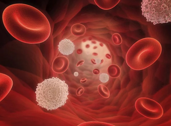
Red blood cells with white cell ~ 2-5 µm
ATP - synthesis, Diameter ~10 nm
The atoms of silicon spacing ~tenths of nm

The Diameter of DNA ~2-12 nm:

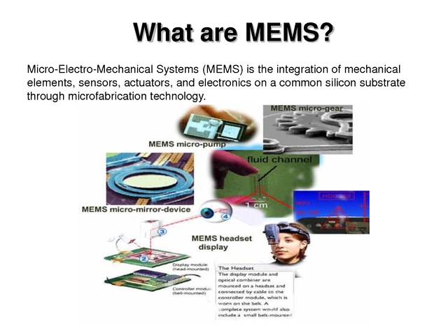
Micro-Electro-Mechanical (MEMS) devices 10 -100 µm:
Pollen grain Red blood cells:

Area x-ray "Lena" the outer ring of the spaces of 35 nm

Self-assembled, structure inspired by nature many 10s nm:
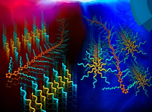
Nanotube-electrode:
Quantumcorral of 48 ironatoms on copper surface positioned one at a time with an STM tip Corral diameter 14 nm:

Fabricate and combine nanoscale
building blocks to make useful devices,e.g.,
photosynthetic reaction center with integral semiconductor storage.

What is nanotechnology ?
Technology on the scale of 10-9m
Nanotechnology is the understanding and control of matter
with dimensions of roughly 1-100 nm, where unique phenomena enable
new application. Nanometer-10-9 of a meter; a sheet of paper with a thickness of about 100 000 nm.
Covering nanoscale science, engineering and technology, nanotechnology
enables visualization, measurement, modeling, and manipulation of matter of that length scale.
At this level, the physical, chemical and biological properties of the materials
differ in fundamental and valuable ways from the properties as individual atoms
and molecules, and volume question. R & D nanotechnology is aimed at understanding and
to create better materials, devices and systems that use these new properties.
The national nanotechnology initiative is a strategic plan.
The unique properties of nanotechnology come from: small dimensions,
including high speed and high functional density (nanoelectronics,
lab-on-chip), small and light weight devices and sensors (smart dust), high
sensitivity (sensors, nanowires) and special surface effects (such as Lotus effect)
very large surface area, providing reinforcement and catalytic action
quantum effects such as high-performance optical fluorescent quantum dot
new molecular structures with new material properties: high strength
nanotubes, nanofibers and nanocomposites.
Downward:
Nanostructures can be made by two complementary approaches.
With top-down technology of nanostructures and devices made
by scaling and miniaturization. It requires precision engineering
down to nano-scale, usually by lithographic patterning,
embossing or imprint techniques with subsequent steps of etching and coating.
Examples:
Micro-and nanoelectronics, MEMS, micro-Electromechanical
nanostructure systems such as Lotus coatings, catalytic
surfaces and membranes, nanostructured coatings in displays,
solar cells, flat batteries nanofibers by electrospinning method nanoglide of the platelets and tubes peeling.
Bottom-up:
The other complementary route is bottom-up, building
nanostructures based on atom-by-atom or molecule - bymolecule mechanical engineering.
It usually requires wet-chemical or steam-phase treatment routes, such as
deposition of an atomic layer. In some cases, the atomic or molecular manipulation
applied through optical, electrical or mechanical nanoprobes.
Typical example:
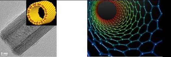
Carbon nanotubes by gas phase deposition nanowires
made from metal, metaloxide, ceramic or even. Type of polymer
by gas-phase deposition method quantum dot is self collecting,
molecular and biostructures of nanomedicine.
Why nano ?
The miniaturisation down to micro & nano level not only leads
to smaller products suited for mass production and lower costs,
it also includes completely new functionalities that cannot be obtained.
at the macrolevel. The new functionality of the acquired physical and chemical
by the effects of small dimensions, the ability to produce new atomic structures,
controllability of very small volumes and coefficient effect on the natural environment.
Small size: mm > µm > nm
Going to small dimensions offers a large number of benefits
for electronic and sensor devices: high functional density:
nanoelectronics, high density memory possible integration of functions: sensing,
DSP, radio, memory and power can be integrated efficient and fast electronic, optical,
thermal and material transportation for mass production with low
cost lightweight, portable, everywhere, everywhere available.
From the material point of view, small dimensions give new
such as: control at the nanoscale enables perfect,
free of structural defects, with exceptional properties for durability, electrical conductivity
etc. nanostructures and particles create a very large surface area, featuring a unique
surface activity for sensing, catalysis, absorption etc.
completely new particles, unknown in nature, can be produced
with new properties, such as carbon nanotubes at nanoscale
quantum effects can be used to obtain
new optical effects.
Small volume: µl > NL > PL
A small volume is especially advantageous for fluidic devices
as measurement devices and chemical processors because of them: fast
response high throughput multi parallel analysis,
matrix single cell / molecule detection of less chemical waste.
A high ratio of the sensor-sample
Scaling of sensor devices to the nano level brings
sensing element in the same dimensional range as the elements being
detected. As a result: high sensitivity high signal-to-noise ratios.
Where in the development of nanotechnology ?
All over the world work on nanotechnology nanotechnology Penn
a very strong innovation driver and is therefore seen as strategic
technology is the economy of the future world. This perception is present all over the world and many
countries are investing in nanotechnology snail funding through the national
or transnational programs in the field of nanotechnology
sauce expectations.
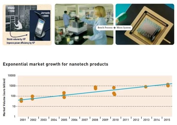
Nanotechnology products Market will grow exponentially.
Analytical place that the market of goods van nanotechnology
can wire sat up to several billion by 2010 and revise one trillion after.
Nanotechnology is expected to get it on almost all technological
sectors as a "enabling" or " key " technology, particularly:
medicine and health
information technology
energy production and storage
transport, vehicles and infrastructure
science material
to prove, water and environment
tool
security.
Next to the ongoing advances in nanoelectronics,
expectations are particularly high for: nano-bio-sensors applications
based on nano and nanomaterials in the long term (10 years).
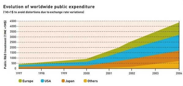
Public investment shows 40% growth annually
Global public investments in R & d increased by 40% last
years and a meek level of € 4,500 million in 2004. Top 6 investors
(2003) with an indication of their direction, are:
Europe: elk, medicine, materials~1250 million euros
USA: all aspects of nanotechnology~1200 million euros
Japan: elk, nanomaterials, nanotubes~750 Euro
C-CORI: high memory density, display~250 million euros
China: mass production of nanomaterials~400 million euros
Taiwan: a display all e - ~ € 150 million
others: various~150 million euros
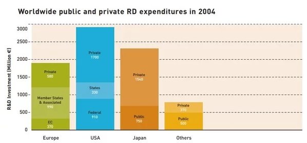
Doubled R & d Investments :
Private global expenditures are at the same level,
that now and public investment. The leader in this field
are USA and Japan (from 1700 and 1540 million euros in 2004 ),
and then Europe and China (€580 and € 370 million private).
This technology. This is a new Era for all Innovative technologies.
Put your fingers up. Click to share it on social networks.
I wish you pleasant travels to the world of technological breakthroughs.
If this article you will interesting. I have a sequel.
From 12 parts of on the subject. Write comments, put likes.
And then I will once a day release the 2nd part of this material.
Thank you for your attention. Don't forget to subscribe to me. And all just the most the most.