剑桥博士再发震撼长文:美国搬起石头砸自己的脚,封杀反而促使华为成长
美国将华为列入黑名单之后,在美版知乎上有人提出一个中国人和美国人都十分关心的话题:
美国将华为列入黑名是典型的中兴式的外科手术式的精准攻击,而且华为似乎已经死了。华为或中国能采取哪些手段来克服这一点或进行报复?中国会怎么做?
在这个问题的留言板里,Janus Dongye Qimeng博士的答案获赞最高,内容最详实。我们先看看这个博士的资料:英国剑桥大学博士,他对地缘政治很感兴趣。
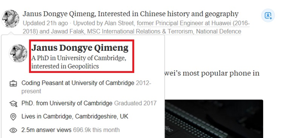
笔者翻了翻他在Quora上的回答问题列表,发现他回答的大部分问题都和中美关系有关,而让Janus博士一答成名的问题则是这个:

这个问题的点赞数高达24.8K,而且中国国内许多媒体都曾经转载过这篇文章。
回归正题,让我们一起看看博士是如何看待美国封杀华为这个事件的。
首先,博士第一句话是:“让我们看看事实,而不是观点。”,然后介绍了华为P30。
Let me introduce the whole supply chain of Huawei’s most popular phone in 2019: P30.
The “brain” of the Huawei P30 mobile phone is called Kirin 980 System-on-Chip designed by HiSilicon. And HiSilicon is the sub-company under Huawei. Why is it called System-on-Chip? Because it is a chip that contains many components designed by the rest of the world and put together in a single chip.
So what is inside the System-on-Chip?
让我来介绍一下2019年在华为整个供应链里最受欢迎的手机:华为P30。华为P30手机的“大脑”被称为麒麟980系统芯片,由HiSilicon设计。海思半导体是华为旗下的子公司。为什么称之为片上系统?因为它是一个芯片,包含了许多由世界其他地方设计的组件,并把它们放在一个芯片上。
那么芯片系统内部是什么呢?
- Instruction set architecture: HiSilicon purchased the CPU and GPU architectural license from ARM in Cambridge, UK. With the license, HiSilicon can use the ARM instruction set (armv8) and develop their own 64-bit CPU architecture. And the bus standard such as AMBA is also licensed from ARM.
指令集架构:HiSilicon从英国剑桥的ARM购买了CPU和GPU架构许可。有了许可证,HiSilicon可以使用ARM指令集(armv8)并开发自己的64位CPU架构。像AMBA这样的总线标准也是由ARM授权的。
笔者要补充一句,V8架构华为已经签署了终身授权,所以不影响现有技术的开发,但是未来V9架构出现之后还没解禁,这会对华为竞争力产生不利影响。 - CPU, GPU: HiSilicon employs several hundred people in Shenzhen, China to design their custom CPU cores, accelerators, and IP components. In order to design their own CPU, they need to use Electronic design automation (EDA) tools from Synopsis, Cadence, and Xilinx. These EDA companies are all American companies in California, USA. HiSilicon needs to pay them license fees to use their tools to design and simulate their own CPUs.
CPU, GPU:在中国深圳,海斯力康雇佣了数百名员工来设计他们定制的CPU核心,加速器和IP组件。为了设计自己的CPU,他们需要使用来自Synopsis、Cadence和Xilinx的电子设计自动化(EDA)工具。这些EDA公司都是美国加州的美国公司。HiSilicon需要向他们支付许可费,让他们使用自己的工具来设计和模拟自己的cpu。
Meanwhile, HiSilicon can also integrate existing softcore designed by ARM, such as powerful core Cortex A76 and power efficient core Cortex A55. Both are in the same chip. The big core is designed in Austin, Texas, USA and the small core is designed in Cambridge, UK. Some of the low-end CPU cores are also purchased from MediaTek in Taiwan. Meanwhile, HiSilicon can also purchase other intellectual properties from ARM including the Mali T830 GPU and the interconnect subsystems. Mali GPU is designed in the ARM headquarters in Cambridge, UK.
同时,HiSilicon还可以集成ARM设计的现有软核,如功能强大的core Cortex A76和功能强大的core Cortex A55。两者都在同一个芯片上。大核在美国德克萨斯州奥斯汀市设计,小核在英国剑桥市设计。一些低端CPU核心也购自台湾联发科。同时,HiSilicon还可以从ARM购买其他知识产权,包括Mali T830 GPU和interconnect子系统。Mali GPU是在英国剑桥ARM总部设计的。 - Memory: HiSilicon designed their own logic in the memory controller and SRAM systems. SRAM and DRAM cells are licensed from Samsung, Korea. The future 7nm 3D stacked RAM would also be designed from Samsung but manufactured in Dalian, China.
内存:HiSilicon在内存控制器和SRAM系统中设计了自己的逻辑。SRAM和DRAM电池均由韩国三星授权。未来的7nm 3D堆叠RAM也将由三星设计,但在中国大连生产。 - DSP & Camera: HiSilicon purchased the Camera lens design IP and control system from Leica Camera from Germany, where most of the system was designed in Wetzlar, Germany. And the actual lens is manufactured by Largan Precision in Taiwan and Sunny Optical Technology in mainland China. The electrical motors for driving camera to change focus is manufactured by Mitsumi in Tsurumaki, Japan. To translate light into signals, the photosensitive film is designed by O-film in Shenzhen, China (also supplier for iPhone X). HiSilicon purchased the hardware solutions for auto-focus and image stabilization from ON Semiconductors in Phoenix, Arizona, USA. The HD video processing chip is licensed from Sony, Japan. And HiSilicon designed their own image processing hardware accelerators (ISP), purchased many DSP IP patents from CEVA in California, USA and AI chips from Cambricon Technologies from Beijing, China.
DSP与摄像头:HiSilicon从德国徕卡相机购买相机镜头设计IP与控制系统,该系统大部分设计在德国韦茨拉尔。这些镜头实际由台湾拉根精密和中国大陆阳光光学科技制造。驱动相机对焦的电机由日本鹤崎三美制造。为了将光转换成信号,这种光敏薄膜由中国深圳的O-film公司(也是iPhone X的供应商)设计。HD视频处理芯片是日本索尼公司授权生产的。海斯力康设计了自己的图像处理硬件加速器(ISP),从美国加州CEVA公司购买了许多DSP IP专利,从中国北京Cambricon Technologies公司购买了AI芯片。 - Baseband: HiSilicon purchased IP license to use WIFI, GPS and Bluetooth IP from Broadcom from San Jose, California. For the 3G support, HiSilicon has to pay a royalty fee to patents held by Qualcomm from San Diego, California. For later 4G LTE and 5G, HiSilicon has its own patents and baseband processor called Balong, which was designed by several hundred people across China. HiSilicon has also purchased the Beidou Navigation system from Chinese Academy of Sciences. Note that some of the chip verification tasks are performed by Indian Engineers in Hyderabad, India.
基带:HiSilicon从加利福尼亚州圣何塞的Broadcom购买了使用WIFI、GPS和蓝牙IP的IP许可证。为了获得3G支持,HiSilicon必须向高通在加州圣地亚哥持有的专利支付专利费。对于后来的4G LTE和5G,海斯力有自己的专利和基带处理器,名为巴隆(Balong),由中国各地数百人设计。海斯力康还从中国科学院购买了北斗导航系统。注意,一些芯片验证任务是由印度海得拉巴的工程师完成的。
Radio Frequency: To multiplex between various communication signals and amplify analog signals to different wireless frequencies, they need radio frequency integrated circuits (RFICs). Most of the patents in RFIC was held by RF Micro Devices from North Carolina, USA and now became Qorvo after merging with TriQuint. In the RFIC chips, you need a few power amplifiers, high-end capacitors manufactured by Murata Manufacturing in Kyoto, Japan. You also need surface acoustic wave (SAW) sensors designed and manufactured by TST Taiwan and Microgate in Shenzhen. You also need a few silicon-on-insulator switches designed by Skyworks Solutions in the USA and manufactured by Skyworks in China. For the antennas components, they are designed and manufactured by Sunway Co. in Shenzhen and Rosenberger (USA) factories based in Shanghai, China. In the age of 5G, Huawei analog devices have to use these devices from the USA, Japan, and China as well.
射频:为了在各种通信信号之间进行多路复用,将模拟信号放大到不同的无线频率,需要射频集成电路(RFICs)。RFIC的大部分专利由美国北卡罗莱纳州的RF Micro Devices持有,与TriQuint合并后成为Qorvo。在RFIC芯片中,需要一些功率放大器,由日本京都村田制造的高端电容器。您还需要由台湾TST公司和深圳Microgate公司设计制造的表面声波传感器。您还需要一些由Skyworks Solutions在美国设计并由Skyworks在中国制造的绝缘硅开关。天线组件由深圳森威公司和中国上海罗森伯格(美国)工厂设计和制造。在5G时代,华为的模拟设备也必须使用来自美国、日本和中国的这些设备。
6.NFC & Touch: NXP Semiconductors in the Netherland provide NFC solutions for Huawei. And the chip is developed by Infineon in Simens, Germany. Goodix Co in Shenzhen provides the fingerprint sensor. USB Type-C solutions are provided by Shenzhen Everwin Precision.
NFC & Touch:荷兰NXP半导体为华为提供NFC解决方案。该芯片由英飞凌公司在德国西门子开发。深圳固迪克斯公司提供指纹传感器。USB Type-C解决方案由深圳恒赢精密提供。 - Fabrication: After HiSilicon integrating all the soft IP and package into one SOC, the design is sent to Taiwan Semiconductor Manufacturing Company (TSMC) in Taiwan for physical layout and fabrication. The fabrication process of the SOC chip is a very complex task. For the most important steps, TSMC needs to import mask alignment systems (MAS) designed by ASML from the Netherlands. They also need to use a lot of wafer chemicals from Shin-Etsu in Japan, Siltronic AG from Germany and SUMCO Corporation from Minato in Japan.
制作:海赛龙将所有软IP和封装成一个SOC后,将设计送至台湾台积电(TSMC)进行物理布局和制作。SOC芯片的制作过程是一个非常复杂的任务。对于最重要的步骤,台积电需要从荷兰进口ASML设计的掩模对准系统(MAS)。他们还需要使用大量的晶圆化学品从日本的Shin-Etsu公司,德国的Siltronic AG公司和日本的UMCO公司。 - Material: However, most of the chemical products and semi-products are imported from China. The most representative one is the rare earth metals in China. For other materials including glasses and steel, BYD in Shenzhen is responsible for manufacturing mobile phone gradient frames and high-density glasses. Shengyi Electronics produces all the PCB board for the phone.
材料:但是大部分化工产品和半成品都是从中国进口的。其中最具代表性的是中国的稀土金属。对于眼镜、钢材等其他材料,深圳比亚迪负责制造手机梯度框架和高密度眼镜。胜益电子为手机生产所有的PCB板。 - Screen: Huawei P30 used Samsung OLED rigid screen but P30 Pro used the OLED soft screen designed by BOE Technology in China. Some screens are also manufactured by LG, Korea and manufactured in Guangzhou, China. Now both Korean and Chinese companies are dominating in the screen market.
屏幕:华为P30采用三星OLED硬屏,而P30 Pro采用京东方科技在中国设计的OLED软屏。一些屏幕也由韩国LG生产,在中国广州生产。现在,韩国和中国公司都在屏幕市场占据主导地位。 - Assemble: Huawei then orders all the components from each service provider and ship the components to Foxconn in Zhengzhou, China. Workers in Foxconn assemble all the components together into one complete phone.
组装:然后,华为从每个服务提供商订购所有组件,并将这些组件运送到中国郑州的富士康。富士康的工人将所有部件组装成一部完整的手机。
Janus博士指出,这些供应商有很多来自美国、中国、日本和韩国,这意味着如果美国杀华为,那么大多数供应商也会受到很大伤害,而且其中大多数是韩国和日本仅存的高价值公司,并且这将对韩国和日本经济造成巨大打击。而且他猜测特朗普背后的人并不懂半导体工业体系。
最重要两个问题是Is Huawei dead? (华为死了吗?)和What would China do?(中国会怎么做?)
华为会死吗?当然不会。十年前,华为已经从美国政府那里启动了各种方案的备份计划。当整个中国都被禁止使用x86指令集时,他们甚至有极端的备份计划。
中国会怎么做? 这将再次为中国创造了一个黄金机遇。如果华为找不到来自美国的供应商,他们就会找到替代品,尤其是中国国内的供应商。这将给国内企业带来巨大的提振,因为它们突然获得了大客户。
看看评论区都说了什么:
现实的美国的纳税人和企业,包括非常脆弱的农民,正在为关税买单和将为关税买单。华为能够挺过这场风暴(显然,我们是唯一一个声称华为存在安全问题的国家和在推出5G方面拥有最好/最便宜的设备,在亚洲手机市场占据了巨大份额)。特朗普只是在激怒中国人。同时,他们的“一带一路”政策正在利用世界各地的反美情绪在世界的各个地方(记住,特朗普的贸易战包括世界其他地区、欧盟、加拿大,以及边界以南的所有国家), 所以他们都对与中国达成新协议持非常开放的态度……中国在反特朗普情绪方面正在取得进展。他们很好,最后,我们输得很大。
中产阶级的我,我们的退休储蓄(我们和我们的退休储蓄都在市场上,不只是富人). 自从特朗普开始说这些废话以来,我们的退休储蓄减少了7.5万美元。普通人,这是10年的辛苦积蓄的替代品!!
华为离死亡还很远,中国政府不会允许任何外国人杀死它,即使是像特朗普这样聪明、有经验的人。他们(华为)将继续努力主导5G市场,在政府的支持下,看起来至少将成为非洲的首选供应商。