Why are semiconductors used in electronics?

Semiconductor technology is present in almost every area of modern day technology and as such semiconductor theory is a very important element of electronics.
In the realization of electronic circuits and systems, primarily are used semiconducting electronic elements whose work is based on the current flowing through the semiconductor. Semiconductors are a group of materials with specific conductivity lesser than specific conductivity of conductors and greater than specific conductivity of isolators. Basic property of semiconductor, which laid foundation for their widespread use in electronics, is the possibility to adjust specific conductivity in wide limits, whether through the change of composition of materials, or using the outer influences.
Electrical properties of material

Properties of solids are defined by the arrangement of atoms or groups of atoms. With the regular arrangement of atoms the material is a crystal, and if arrangement irregular we are talking about amorphous material. Crystal materials can be either monocrystalline, with regular arrangement of atoms in the whole volume or polycrystalline, which consist of large number of monocrystalline grains. Regularity of the arrangement of atoms inside a grain is broken on the brain borders.
Electrical properties of material are defined by their atomic structure. Atoms consist of positively charged nucleus and negatively charged electrons which orbit around nucleus. Electrons have discrete energies. When crystal is formed, consisting of large number of close atoms, discrete energy states of individual atoms merge in to the energy band with permitted electron energies.
Material conductivity is defined by the electrons that have weakest bounds to the nucleus, called valence electrons.
On the temperature of absolute zero ( T = 0 K = -273 °C) all of the electrons are tied to the nucleus. Because of the lack of movable electrons, as charge carriers, there can be no current flow.
![]()
Increase in the temperature results in increased thermal energy of electrons. At the temperature T > 0 K part of the valence electrons acquires enough energy and frees itself from the atom nucleus. Energies of free electrons correspond to the energies of conduction band. Energies of conduction band are greater than energies of the valence band. Minimum energy required for release of atom is the difference between highest energy of valence band and lowest energy of conduction band. Difference matches the width of the forbidden band. Electrons can't have energy values inside of forbidden band. Free electrons from the conduction band can move through the crystal structure and partake in the current flow.

The difference in electrical conductivity of material is defined as the energy necessary for releasing electron from valence band, i.e. the amount of free electrons in the conductive band. In the conductor, valence and conduction band are overlapping and on the temperature T > 0 K practically all of the valence electrons are free. Because of the great concentration of free electrons, specific conductivity of the conductor is big.

In semiconductors and isolators valence and conduction band are separated by the forbidden band. At room temperature thermal energy of electron is insufficient for its transition from valence to conduction band. Consequently, the lack of free electrons in conduction band disables the current flow. Width of the forbidden band in semiconductors is around few electronvolts.
Silicon structure
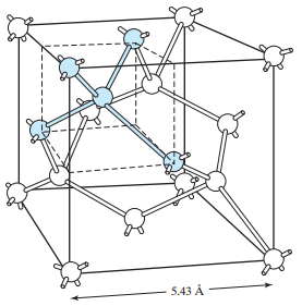
Most frequently used semiconductor material in electronics is silicon (Si). As a tetravalent element silicon has four valence electrons. Silicon atoms are tied together in a crystal structure, called diamond structure, with the arrangement in which every atoms is in the center of the tetrahedron, and four neighbouring lie in its apexes. In between the atoms a covalent bond is formed. Through that bond, each atom shares its four valence electrons with neighbouring atoms, pairing the electrons.
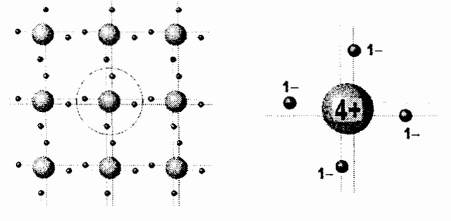
For the sake of simplicity a flatbed view of the crystal structure is showed. Central part of each atom includes nucleus and all of the electrons except the four valence ones. Valence electrons, symbolized by the filled circles, form pairs between the neighbouring atoms.
Pure silicon
![]()
At the temperature T > 0 K part of the valence electron acquires sufficient energy for abortion of the valence bond and frees itself from the mother atom, which corresponds to jump from the valence to conduction band in energy diagram. In the position of broken valence bond there is a lack of electron, i.e. a hole. Hole is easily filled with an electron from the neighbouring valence bond, therefore the hole is moving to its spot and whole procedure is repeated.
Along with the movement of free electrons, in silicon crystal we can also observe movement of valence electron across the holes of broken valence bonds. Series of electron jumps across the hole spots can be observed in a simpler fashion, as a movement of holes in the opposite direction. Because at the hole location there is a lack of electrically negative electron, charge of the hole is positive, and equal to the electron's charge value.
Consequently, electrical current flow in semiconductor is lead by two types of carriers - free electrons of the conduction band and holes of valence band.
In pure silicon the number of free electrons in conduction band is equal to the number of holes in valence band. Pure silicon is called intrinsic silicon, and accompanying concentration of carriers is intrinsic concentration. At room temperature intrinsic concentration is extremely small in comparison to concentration of silicon atom, therefore specific conductivity of pure silicon is low and borders with the conductivity of an isolator.
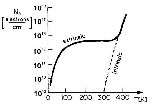
Conductivity of pure silicon varies significantly with the change of temperature. Increasing the temperature results in increased number of electrons capable to break the valence bond, resulting in the increase of carrier concentration and conduction of pure silicon. Conductivity of the pure silicon can also be increased by other external influences, which use energy to free the pairs of free electrons and holes. For example, electromagnetic radiation.
Doped silicon
Specific conductivity of semiconductor elements is adjusted by doping, i.e. addition of atoms of specific impurity elements in the material structure. Impurities that change the semiconductor conductivity are elements whose valency is greater or lower than the valency of semiconductor valency by 1. In silicon impurities are therefore either three or five-valent, i.e. elements with three or five valency electrons.
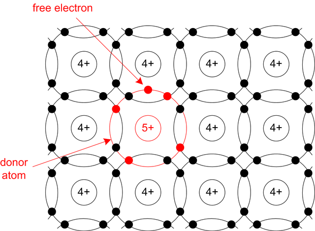
As a five-valent impurities are used phosphorus (P), arsenic (As) or antimony (Sb). Four valency electrons of these atoms establish a connection with four neighbouring silicon atoms. Fifth electron is loosely tied to its atom. Energy necessary for breaking up the bond between atom and fifth electron is small and at room temperature practically all of the fifth electrons are free. Freeing, fifth electron can move through the material. With releasing one electron in conduction band atoms of the five-valent element become positive ions. Five-valent atom gives a free electron and therefore is called donor.
Silicon doped with donor impurities has significantly greater concentration of free electrons than the concentration of holes. Electrons are majority and holes are minority carriers. As the current mostly consists of negatively charged electrons this type of silicon is called n-type.
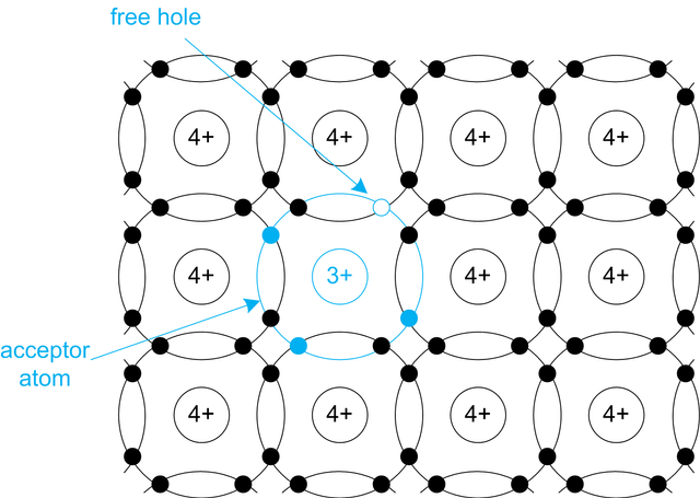
Adding the three-valent atom (most often Bohr - B) crystal structure of silicon acts differently. Three valency electrons of three-valent atom establish a connection with three neighbouring atoms of silicon. Connection to one of the silicon atom stays unfilled. On that spot a hole is present. In unfilled bond a valency electron from the neighbouring bond is easily transffered, consequently creating the hole on its original position. That way a movement of holes through the valency electrons is achieved. Accepting the electron, bohr atom is ionized, becoming negatively charged. Three-valent atom is called acceptor.
In this case hole are majority, and electrons are minority carriers. Material is characterized by positive holes and therefore is called p-type silicon.
Semiconductor doped with impurities is also called impure or extrinsic semiconductor.
Summary
In solid-state physics, a band gap, also called an energy gap or bandgap, is an energy range in a solid where no electron states can exist. It is the energy required to promote a valence electron bound to an atom to become a conduction electron, which is free to move within the crystal lattice and serve as a charge carrier to conduct electric current.
![]()
In semiconductor production, doping intentionally introduces impurities into an extremely pure intrinsic semiconductor for the purpose of modulating its electrical properties. The impurities are dependent upon the type of semiconductor and the properties that it needs to have for its intended purpose. Lightly and moderately doped semiconductors are referred to as extrinsic semiconductors. A semiconductor doped to such high levels that it acts more like a conductor than a semiconductor is referred to as a degenerate semiconductor.
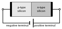
In the next post I will write about semiconductor diode and why it is at the very centre of much of today's electronics industry.
Thank you for reading and feel free to provide feedback.
GREAT article and very clear info. thank you for the quality, time and dedication. Namaste :)
Wow! This was really informative, thank you for the info!
This reminds me the classes I took at the university ^^
Thanks for sharing!
This is great. Thanks for the information :)