DIY: Making a Printed Circuit Board (PCB) at Home
My friend designs and builds inverters and other electronics. Today, I was around when he started building one. But first, he had to make a Printed Circuit Board known popularly as PCB.
He first started by making a PCB design using Sprint Layout 6.0 Software.

Screenshot showing the PCB design done on Sprint Layout 6.0 Software
There is other available software for this PCB design like Eagle, Proteus, etc. For this design, he used Sprint 6.0
The red lines indicate the top of the PCB, while the green part indicates the bottom side of the board. The bottom side is where the copper that is used for via, tracks, etc. are connected.
Via: Vertical Interconnect Access, that is a hole that is electrically connected so current can pass through it.
Pads: small copper surface where electronic components are soldered.
Tracks: a copper conducting path (lines) for connecting two points.
Next is to print it out the PCB design on a special glossy paper.

PCB printed on a glossy paper
Prepare the copper-clad board by degreasing (grease removal) by using emery cloths or a razor blade or any solvent that can remove grease. It is important to do that to remove any impurity from the copper board's surface. This is because copper coating easily gets oxidised when exposed to air and moisture.
Transfer the PCB design printed out on glossy paper to the copper board via heat transfer. This he achieved by using a hot pressing iron on the glossy paper placed on the copper board.

Transferring design of PCB to copper board via heat from pressing iron
The toner is then imprinted on the board in the way the PCB was designed. Toner is etch-solution resistant.
The next step involves soaking the board in water to make for easy removal of the irrelevant portion of the glossy paper sticking on the copper board.

Toner is transferred to the copper board and would shield areas that it is on from being removed by the etching solution
Check the PCB design for broken lines or place the toner did not cover well. That leaves some useful part of the board exposed and will be removed when dipped in the etching solution. Cover such places with either of these: an etching pen, permanent marker, nail polish, oil paint or any etch-resisting solution available.
Now the etching begins. Dip the copper board into a warm solution of ferric chloride (FeCl3) which is the etching solution. The solution works best if hot. That can be done by mixing the ferric chloride powder with warm water.

A solution of ferric chloride used as the etching solution
Caution: Always pour (FeCl3) power into the water and not water into the (FeCl3) to reduce the excitation that would occur when you do that. Always wear eye goggles for safety.
Gently move the etching solution with the board inside it to ensure an even etching process.
Wash the PCB board thoroughly with water. Use thinner to wash after to remove any other etch-resisting material on the board. The board is now ready to have components placed on it.
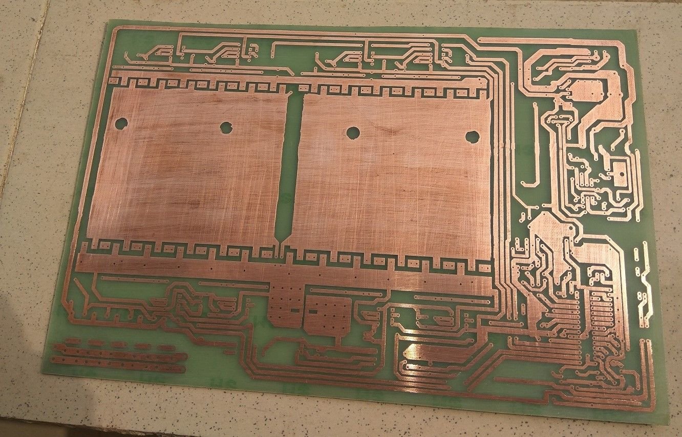
A PCB ready for components
All images were taken with my mobile phone.
Thanks for reading

nice share Do it yourself is always a great idea. and you made printed circuit board so easy. keep sharing nice stuff @greenrun
Thank you.
This is a great initiative! I used SteemData for my two sites Steem-Buddy and Steem-Flow so I help when ever I can. Upvote, Resteemd, and Tweeted @bijoy123
Wow! This is an interesting technical experience. Good job.
Thank you.
Good jop friend
The way you analyse the whole thing here can even help a layman to understand and wanna try it out. Kudos to your intellect
Thanks for the compliments. I'm blushing here :)
Wow. Didn't know one could build home made PCB. Usually thought only companies could do it. Nice post
No, you could make one at home.
Never knew these stuffs could be made in Nigeria. Big ups to you. I don't mind investing in your company if you have one.
It could be made any place. Thanks.
@greenrun what tool is use to remove the unwanted part of the copper board.
I mentioned it in the post; he used a ferric chloride solution to do the etching.
Ok
main board information!
Thanks a lot
another interesting stuff. A bit of eye opening for a lay man like me when it comes to electronics
Oh yeah. Thanks a lot