Bulldozer from AMD vs. INTEL! A state of Zen: AMD unveils new architectural details on its latest CPU core
AMD unveiled a great deal of information at Hot Chips about its upcoming “Zen” CPU core and architecture. The new chip has been the subject of an enormous amount of speculation for more than a year, but things have heated up over the past few weeks as leaked benchmarks surfaced and AMD conducted its own public test.
Today’s information dump is the most detail AMD has shared to date — in fact, it’s significantly more information than I expected the company to share until Zen actually launched. Let’s get started.
Zen’s design goals
Zen is best understood as a response to the problems that plagued Bulldozer. AMD’s original goal with that architecture was to intelligently share resources between CPU cores, while simultaneously hitting higher frequencies and higher execution efficiencies than AMD’s previous CPU core, K10. Bulldozer’s failure to deliver left AMD in an ugly position: Should it try to repair its old core or return to the drawing board and build something completely new?
Sources we’ve spoken to at AMD suggest that the difficulty of repairing Bulldozer was significant enough that AMD opted to build a new core from scratch with none of Bulldozer’s baggage. That doesn’t mean there’s no Bulldozer DNA in Zen — in fact, AMD has stated that the expertise it gained from improving Steamroller and Excavator’s energy efficiency was put to good use for its newest architecture. Say instead that what design elements AMD does borrow from its previous architectures will be the components of the chip that actually worked well rather than the problematic ones that dominated its performance.
Cache architecture
Much of what went wrong with Bulldozer was linked to its cache subsystem and overall architecture, so that’s a good place to start diving into Zen.
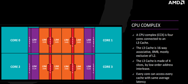
Where Bulldozer used the concept of a CPU module (defined as a pair of cores that shared resources), Zen uses complexes. One CPU complex (CCX) contains four cores, 2MB of L2 cache (512KB per core), and 8MB of L3 cache. That means AMD’s highest-end consumer Zen contains eight cores and 16MB of L3 cache in total, split into 2x8MB chunks. AMD has stated that the two CCXs on an eight-core chip can communicate with each other via the on-chip fabric, though there’s likely a performance penalty for doing so.
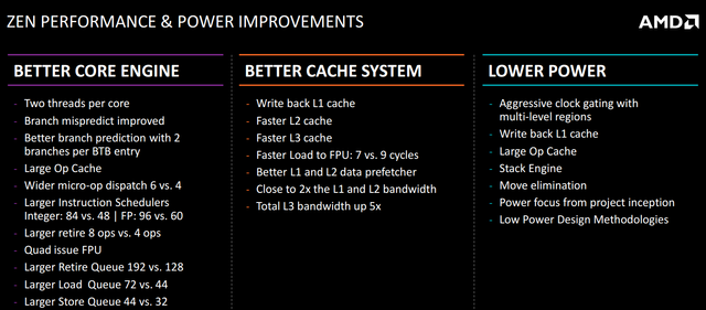
Zen’s L3 cache operates as a victim cache for the L1 and L2, meaning data evicted from those caches is stored in the L3 instead. It’s also 16-way associative, which is a significant change from Bulldozer’s 64-way associative L3. A cache with a higher set associativity has a greater likelihood of containing the information the CPU is looking for, but takes longer to search — and one of the issues that crippled Bulldozer was its cache latency at nearly every stage.
We don’t know anything about clock speeds on either the L3 cache or the integrated memory controller. Historically, AMD’s Bulldozer-derived CPUs and APUs have used a clock between 1.8 – 2.2GHz for the L3 cache and IMC.
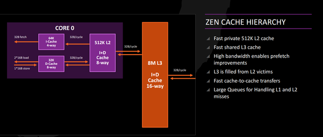
AMD has stated that L1 and L2 bandwidth is nearly 2x Excavator while L3 bandwidth is supposedly 5x higher. These changes should keep the core fed and support higher performance. The L1 cache is write-back instead of write-through — that’s a significant change that should improve performance and reduce cache contention (Bulldozer’s write-through cache meant that L1 performance could be constrained by L2 cache write speed in some cases).
The CPU core
We’ve already tackled caches, so let’s check out the CPU core itself.
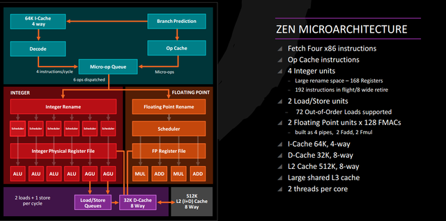
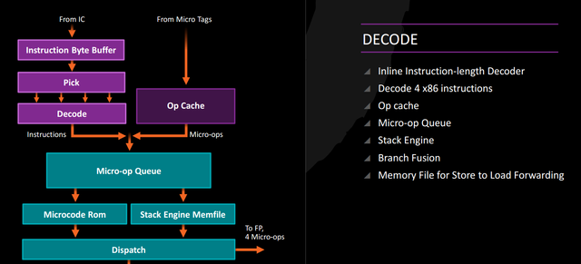
Here’s Zen’s high-level core diagram. There are several significant differences compared with AMD’s older Bulldozer core, including the addition of an op cache, a micro-op queue, and a larger number of integer pipelines per core.
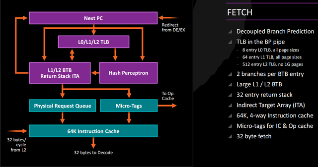
Here’s an expanded view of how the core gets fed. This was another major problem area with Bulldozer — Bulldozer and Piledriver’s shared logic meant that the dispatch unit could only send work to one core or the other every clock cycle. Steamroller later fixed this issue by doubling up dispatch units, but this only resulted in a modest performance improvement.
AMD has taken a page from Intel’s book and implemented an op cache with Zen, even if we don’t know much about the specifics of the feature. This allows the CPU to cache decoded operations that it may need to dispatch repeatedly rather than requiring it to repeatedly decode and dispatch the same instructions. Each Zen core can decode four instructions per clock cycle, but the micro-op queue can dispatch six instructions per cycle. Clearly AMD anticipates that its cache will relieve pressure on the decode units and help keep the core fed while reducing power consumption. Steamroller had a macro-op queue that could hold up to 40 macro-ops but its usefulness was limited to tiny loops.
Like the Bulldozer family, Zen can theoretically fetch 32 bytes of data at a time, though CPU analyst Agner Fog found that the Bulldozer family of cores was practically limited to 21 bytes of data when both cores were in use or 16 bytes if one core was used. He theorized that this limit may have been why doubling up on Steamroller’s dispatch units yielded relatively limited results. Resolving this in Zen could be part of why AMD has significantly improved its IPC.
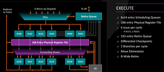
The integer cores have been rebalanced from the Bulldozer family. Prior to Bulldozer, AMD’s K10 paired three ALUs with three AGUs (address generation units). Bulldozer trimmed this to two ALUs and two AGUs per core. This, combined with the limited dispatch ability in the BD/PD cores, was thought to be a major performance bottleneck until Steamroller added additional dispatch capabilities and slashed the penalty Kaveri took when scaling across multiple cores. (Piledriver and Bulldozer achieved roughly 1.8x of the scaling you’d expect from a “true” dual-core, while Steamroller hit approximately 1.9x.) Four ALUs and two AGUs could boost overall performance compared with Bulldozer’s narrow design, but we’ll have to see how the chip performs in benchmarks.
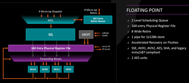
AMD’s floating point unit will still use 128-bit registers for AVX and AVX2, but latency on some FP operations has been decreased and there are now four pipes instead of three to feed the FPU. The CPU isn’t capable of executing 256-bit AVX instructions in a single cycle. Whether this will prove a detriment in real-world code is an open question, but AVX/AVX2 haven’t boosted general application performance the way SSE2 once did.
Putting it all together:
If you want a single high-level slide that captures what AMD has disclosed about Zen to date, this is it:
There are still some areas of the chip I haven’t touched on, like SMT, because I want to research how AMD’s SMT implementation differs from Intel’s but haven’t had time to examine the topic in-depth. AMD hasn’t stated that Zen will use features like Carrizo’s AVFS, but given that they’ve extended that approach across both Polaris and their APU lines it’s a safe bet they will.
Still, there’s a lot here to suggest that Zen will deliver substantially better performance than any Bulldozer core ever did. The devil, as always, will be in the details. How much performance does AMD gain with SMT? What clock speeds can it hit? How will it price the core against Intel’s current products? Will it deliver “enough” of a performance improvement and how will its chipset features compare with what Intel brings to market?
These are important questions that will ultimately determine whether Zen can reignite competition in the CPU market. Speaking strictly for myself, I’m cautiously optimistic about Zen. Bulldozer, in retrospect, was almost perfectly ill-positioned for the realities of the CPU and foundry business from 2011 to 2016. It was a CPU designed for high frequencies at a time when CPU frequency had slammed face-first into fundamental scaling limits. AMD improved the core’s performance and power efficiency but couldn’t fix the problems that broke it in the first place. It’s not ridiculous to think that the company could spin a chip with 40% improved IPC given where they started from.
Zen doesn’t need to match Intel clock-for-clock or core-for-core to be a huge improvement over where AMD is today. It needs to offer improved efficiency, power efficiency, and much more competitive performance at a relevant price point. Based on what AMD has disclosed to-date, I think they’ve got a real chance of pulling it off. And while we thought much the same thing about Bulldozer five years ago, Zen isn’t trying to create a new type of shared-resource CPU. That should count for something in the final analysis.
Zen is expected to debut in Q1 2017 in wide volume. The current smart money is on a CES debut and launch, though that’s just a guess based on previous schedules and product cycles.
Congratulations @nicu! You received a personal award!
You can view your badges on your Steem Board and compare to others on the Steem Ranking
Vote for @Steemitboard as a witness to get one more award and increased upvotes!