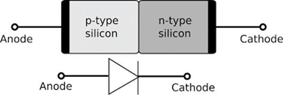
what is P-Njunction diode
A PN junction diode is a semiconductor device formed by joining together a P-type (positively doped) and an N-type (negatively doped) semiconductor material. N-type material has a high concentration of free electrons, while p-type material has a high concentration of holes. Therefore, at the junction, there is a tendency for free electrons to diffuse over to the P side and the holes to the N side. This process is called diffusion.
when an electron diffuses from the n-side to the p-side, a layer of negative charge ion is developed on the p-side of the junction. Similarly, when a hole goes from the p-side to the n-side, a layer of positive charges ion is developed in the n-side of the junction. This creates an electric field in the junction. This electric field further repels electrons flowing into the p-side, and also holes flow towards the n. After some time the equilibrium state will reach and there is no diffusion. This region of positive charge ion and negative charge ion of the junction is termed the depletion region or potential barrier or junction barrier or forbidden layer. The potential barrier is approximately 0.7V for a silicon PN junction and 0.3V for a germanium PN junction. The distance from one side of the barrier to the other side is called the width of the barrier.