The last technological frontier ...
In his post about "Distributed networks of combat modules," I told about the creation by NATO troops of a distributed network for collecting information and destroying targets in the form of combat modules.
Their further development is associated with a decrease in size, the lack of people on board and the increase in the speed of operation of electronic systems. All electronics consists of microprocessors, their work depends on the speed of calculations, reduction of used electric energy and reduction of their sizes.
The one who will create the smallest chip with more performance with less power consumption, he can create autonomous combat modules of smaller size performing tasks without human participation.
If World War II is a war of motors, then the third will be a war of computing systems, the one who will have faster modems and processors will win. In 1947, William Shockley, John Bardeen and Walter Brattein in the Bell Labs laboratories first created an operating bipolar transistor, for which they received the Nobel Prize in Physics in 1956 "for semiconductor research and the discovery of a transistor effect", but MOS (metal oxide semiconductor) the transistor was manufactured only in 1960.
The layout of the field MOS transistor looks like this:
A field effect transistor consists of 3 basic elements: drain, source and gate. The metal gate is separated from the conductive channel between the source and drain by means of a so-called high-k material (or a material with high dielectric permittivity).
This material allows, firstly, to reliably isolate the gate from the channel through which the current flows, and, secondly, to reduce the geometric dimensions of the individual element of the microchip. As such material, to date, use is made of hafnium oxide or silicide, as well as compounds based on them.
The principle of the FET operation is to create a certain potential difference between the gate and the silicon single crystal, depending on the sign of the applied voltage, the current between the drain and the source either flows or does not, i.e. Electrons from the source under the action of the electric field of the gate deviate and do not reach the drain. How to create layers, 3 nm thick, to "paste" drains, sources and closures, in order to finally get a microprocessor?
This procedure consists of several stages. The first stage is the special preparation of quartz sand - its recovery by coke in arc furnaces, where thousands of amperes of electric current heat the surrounding space to a temperature of about 1800 ° C, resulting in the formation of so-called technical silicon:
SiO2 + 2C = Si + 2CO.
Silicon tetrachloride (SiCl4) is obtained by chlorination of technical silicon, which is then converted to trichlorosilane (SiHCl3):
3SiCl4 + 2H2 + Si = 4SiHCl3.
After several more steps, we obtain high purity silicon, only one foreign atom per billion atoms of silicon:
2SiHCl3 = SiH2Cl2 + SiCl4 2SiH2Cl2 = SiH3Cl + SiHCl3 2SiH3Cl = SiH4 + SiH2Cl2 SiH4 = Si + 2H2
After this purification, silicon is melted in special furnaces, and then a huge monocrystal is grown by the Czochralski method, drawing it out melt at a rate of several millimeters per minute. The resulting column weighing more than 100 kg is sawn to thousands of thin (only 1 mm thick) wafers.
Then each such wafer is polished to a mirror shine, and only then do they start forming tens and hundreds of chips on the substrate by means of the lithography process. Immediately before the start of the lithographic process, a thin layer of oxide is formed on the wafer, and an even finer layer of high k material is deposited by magnetron sputtering at high temperature.
Further on, a small amount of a photosensitive polymer drips onto the substrate while rotating, which forms the next thin layer on the surface. Such a polymer is capable of changing its properties under the influence of ultraviolet radiation.Then "wafer" is placed under a special lens system, behind which is a photo mask and a source of laser UV radiation.
Now the robotic system passes hundreds of times along the substrate and leaves "imprints" on it. After the end of this process, the wafer is placed in a solvent, under which the exposed areas of the polymer dissolve and are removed from the plate.
Thus, a three-dimensional relief is formed on the substrate, the "depressions" in this relief are filled with certain substances, and the lithographic process (that is, the exposure of the plate under the laser beam) is repeated several dozen times. In total, to "print" the chip requires several hundred different technological stages, most of which are carried out in super-clean rooms.
So, layer by layer on one side of the "waffle" there is an excellent three-dimensional composition of copper conductors and transistors, which after a short period of time will be cut from the "wafer" and become the heart of the computer.
Until recently, the lithographic process was simple, because the wavelength of the radiation was smaller or comparable with the dimensions of the individual "printed" elements on the substrate. At the turn of the 21 century, the leading manufacturers of microprocessors stepped over, so-called, the diffraction limit, i.e. using a laser with a wavelength of 248 nm, steel chips were produced, the individual elements of which were only 190, 130, 90 nm, which would be unthinkable when using classical optics.
Accordingly, innovative approaches to the design of masks (for example, so-called mask with phase shift) were developed and implemented, and the computing power of computers was developed to design microchips and take into account the wave nature of light.
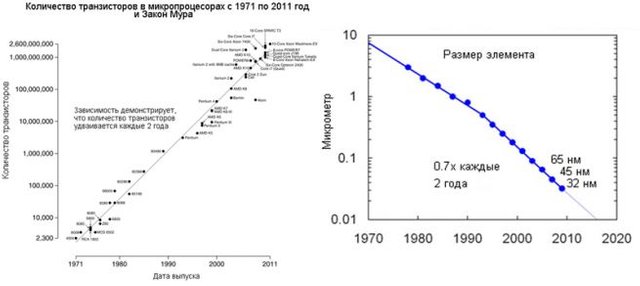
Gordon Moore, preparing his next performance as head of the department of R & D (research and development) company Fairchild Semiconductor, noted an interesting empirical fact: the number of transistors in the chip of the microprocessor doubles every two years.
In July 1968, Moore and Robert Noyce left, their company Fairchild Semiconductors, and founded the corporation Intel.
Several years ago, the miners created a steady demand for ASIKi, whose heart is also microprocessors. So we (I monyu monero) became participants in the arms race. The coining company CoinRage entered the testing phase of the CR10NM10 chip. Previously, the top of the scientific fantasy was the chip CR16NM16, but the last generation managed to bypass it in power.
The previous devices functioned at 16 nm architecture, and the current product allows to reduce purchase costs up to four times, while its performance has almost doubled. This was achieved thanks to the use of 10 nm technology, which made it possible to apply a larger number of crystals and add immersion cooling. The technology of manufacturing microprocessors based on silicon rested on a technological impasse.
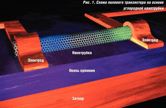
Further reduction in size, increased productivity became impossible and scientists drew attention to graphite nanotubes, allowing to overcome the size limit and create microchips with even greater performance. Developers of microprocessors went in three ways. The transistor is manufactured as follows. A pair of electrodes is applied to the silicon wafer - the drain and the source, between which a nanotube is placed.
The plate itself is a shutter. In the normal state, the channel is closed, because there is a potential barrier for holes. The conduction band and the valence band are separated by a forbidden band with a width of several eV.
If a voltage is applied to the gate, which will lead to the appearance of an electric field where the CNT is located, then its zone diagram is reconstructed, it becomes a good conductor. Thus, by changing the voltage at the gate, it is possible to control the conductivity of the nanotube and accordingly open or lock the transistor.
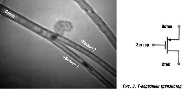
Another group went along the path of creating transistors from hydrocarbon nanotubes.Synthesis of Y-shaped nanotubes, which in themselves can already perform the functions of a transistor, without any additional elements.
To create such structures, nanoparticles of catalytically active titanium are applied to the prepared CNT, which act as a point of growth of the second "branch" on the surface of the already formed tube. When voltage is applied to the "trunk" of a nanotube, the flow of electrons from one branch to the other stops.
As soon as the zero potential of the "trunk" of the nanotransistor is restored, the current flow through the "branches" is resumed. The third group of developers went even further to the problem of creating microprocessors.
Processing a large amount of information requires a request for previously unknown data that has not yet been cached. In this case, it takes a lot of time to execute a new query. The request to receive information for processing a particular command will first go to the internal cache of the processor itself.
Further, after searching all the levels of the cache, an answer will be received that there are no hits and the kernel will send a request to RAM. After searching through the memory, again, there will be an answer that nothing has been found. And only then the request will be sent to the HDD or SSD drive.
The signal will have to pass through relatively thick (for electrons) wires, overcoming the constant resistance. Agree, this way is too long and for this period of time the kernel would have had several times to finish processing.
If you performed this query instead of your PC, then 96% of the time would be waiting. It is also worth remembering that even when the CPU expects the receipt of the required instruction, it still consumes electricity.
As an alternative, you can suggest to combine the CPU and memory on one plate. That's just not possible to place these two components on one plate - silicon wafer requires heating at 1000 degrees C, which will lead to the melting of metal elements of a solid-state drive or hard drive.
Developers of microprocessors went in three ways. The transistor is manufactured as follows. A pair of electrodes is applied to the silicon wafer - the drain and the source, between which a nanotube is placed.
The plate itself is a shutter. In the normal state, the channel is closed, because there is a potential barrier for holes. The conduction band and the valence band are separated by a forbidden band with a width of several eV. If a voltage is applied to the gate, which will lead to the appearance of an electric field where the CNT is located, then its zone diagram is reconstructed, it becomes a good conductor. Thus, by changing the voltage at the gate, it is possible to control the conductivity of the nanotube and accordingly open or lock the transistor.
Another group went along the path of creating transistors from hydrocarbon nanotubes. Synthesis of Y-shaped nanotubes, which in themselves can already perform the functions of a transistor, without any additional elements. To create such structures, nanoparticles of catalytically active titanium are applied to the prepared CNT, which act as a point of growth of the second "branch" on the surface of the already formed tube.
When voltage is applied to the "trunk" of a nanotube, the flow of electrons from one branch to the other stops. As soon as the zero potential of the "trunk" of the nanotransistor is restored, the current flow through the "branches" is resumed. The third group of developers went even further to the problem of creating microprocessors.
Processing a large amount of information requires a request for previously unknown data that has not yet been cached. In this case, it takes a lot of time to execute a new query. The request to receive information for processing a particular command will first go to the internal cache of the processor itself.
Further, after searching all the levels of the cache, an answer will be received that there are no hits and the kernel will send a request to RAM. After searching through the memory, again, there will be an answer that nothing has been found. And only then the request will be sent to the HDD or SSD drive. The signal will have to pass through relatively thick (for electrons) wires, overcoming the constant resistance.
Agree, this way is too long and for this period of time the kernel would have had several times to finish processing. If you performed this query instead of your PC, then 96% of the time would be waiting. It is also worth remembering that even when the CPU expects the receipt of the required instruction, it still consumes electricity.
As an alternative, you can suggest to combine the CPU and memory on one plate. That's just not possible to place these two components on one plate - the silicon waffle requires heating at 1000 degrees C, which will lead to the melting of metal elements of a solid-state drive or hard drive.
To get around the problem with the temperature difference, the Stanford University team turned their attention to the one-dimensional carbon material, carbon nanotubes, discovered about 10 years ago. These are extended cylindrical, mesh structures of carbon atoms with diameters from one to several tens of nanometers.
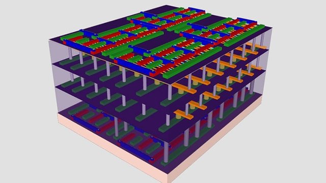
The processing capabilities at low temperature have become key in the choice of material for an alternative to silicon. The processing temperature is only 200 ° C. CNTs (carbon nanotubes) have electrical conductivity properties equal to silicon transistors, but their electrical properties depend on the twisting angle of the hexagonal graphite plane. Now, researchers at Stanford have created a system for stacking memory along with transistor layers, connecting them together.
The new structure significantly saves the time of requests and, accordingly, the time of complete processing of the team. 1000 times faster than similar systems of equal performance. As soon as numerous studies on the creation of microprocessors from carbon nanotubes reach the point of introduction into production, the modern world that we are familiar with will end.
There will be so perfect independent combat modules that humanity will face the threat of self-destruction. No fourth World War with the use of sticks and stones will not, on the planet will remain only insects.
The only salvation for mankind facing an impending and imminent threat is the expansion of the idea of humanism in human minds. If it takes people before the last technological frontier is overcome, then a great and interesting future awaits us.
The first photo with RH, the rest with Google.


This post has received a 0.28 % upvote from @drotto thanks to: @varja.
This post has received a 1.15% UpGoat from @shares. Send at least 0.1 SBD to @shares with a post link in the memo field.
Invest your Steem Power and help minnow at the same time to support our daily curation initiative. Delegate Steem Power (SP) to @shares by clicking one of the following links: 1000 SP, 5000 SP or more. Join us at https://steemchat.com/ discord chat.
Support my owner. Please vote @Yehey as Witness - simply click and vote.
You just rose by 5.4699% upvote from @therising courtesy of @varja. Earn 43.8% APR & rise further by delegating SP to therising. For more details visit: https://steemit.com/budget/@therising/auto-daily-payout-of-43-8-apr-for-steem-power-delegations-starting-from-500-sp-only-limited-period-offer.
This post has been upvoted by @microbot with 3.4%!
Thank you for giving your trust and witness vote to my creator @isnochys!
You got a 0.57% upvote from @mercurybot courtesy of @varja!
This post has received a 19.78 % upvote from @chronocrypto thanks to: @varja.