Design of an amplifier of audio with Qucs
What Will I Learn?
In this tutorial you will learn:
- Work with the transistor BJT, polarization and amplification.
- Analyze the operation of a circuit with transistors using the Qucs.
- Apply the simulation tools of AC, DC signals and parametric sweep of the Qucs.
Requirements
- The user must read the previous tutorials, related to the analysis of electronic devices using the Qucs.
- Possess an intermediate knowledge of the management of semiconductor electronic devices of three terminals.
- Know the mode of operation of the BJT transistors and the analysis of circuits with this type of transistors.
- Know the methods of simulation of Qucs.
Difficulty
- Intermediate
Tutorial Contents
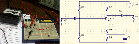
Greetings community Utopian-io, the following tutorial of the account @edagmi, is a material used in the career of electronic engineering in Venezuela, this material allows to design and analyze a voltage amplifier for audio signals, using the Common Emitter configuration with transistors BJT NPN semiconductors. For the design and subsequent analysis, the Qucs electronic circuit simulator will be used, with transient applications to see the response generated by the designed circuit.
We want to design the common emitter amplifier (observe figure), using the Qucs, with an NPN transistor of B = 100 and a gain voltage greater than 15. This circuit can be used to amplify medium frequency audio signals. The following image shows the final circuit that will be generated in this tutorial:
The gains achieved for this circuit are described by the following equation:
AV= gm(R2‖R6)
Where gm is an internal admittance parameter and depends on the polarization current Ic.
The capacitor C1 couples the input AC signal with the DC polarized Common Emitter circuit. In AC, it has an impedance based on the time given by the following equation:
Zc = 1 / (2pi * f * C)
Where f represents the frequency or inverse of the period of the signal.
The following describes the different steps to be performed in the Qucs simulator, to design the Audio Amplifier:
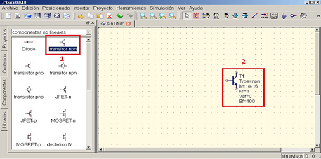
Step 1:
The first thing we must do is select a transistor BJT NPN with a gain factor of beta = 100, in the group of non-linear components we can select the transistor.
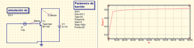
Step 2:
To the selected transistor we must make a steady state analysis or DC, and a sweep of parameters, to be able to visualize the input response of the Common Emitter circuit. For this type of analysis we use a current source and a DC voltage source, to define the polarization values of transistor BJT.
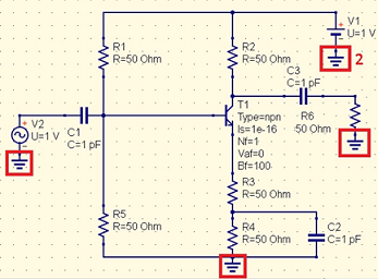
The following picture shows the schematic of the BJT circuit and the input curve of the Common Emitter circuit.
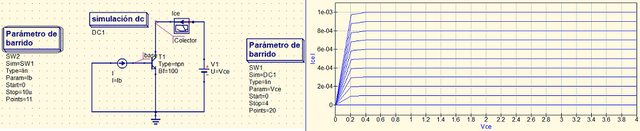
Step 3:
The output curve of the Common Emitter circuit is more complex because it includes the base current to control the output response in conjunction with the collector current and the emitter collector voltage.
Next, a steady state or DC analysis is performed, and two sweeps of parameters, to be able to visualize the output response of the Common Emitter circuit of transistor BJT. A nested sweep is made of the voltage and current sources that polarize the circuit.
The following picture shows the schematic of the BJT circuit and the output curve of the Common Emitter circuit.
The nextlist code of the parametric scans and the schematic for the transistor curves:
<Components>
<_BJT T1 1 470 180 8 -26 0 0 "npn" 1 "1e-16" 0 "1" 0 "1" 0 "0" 0 "0" 0 "0" 0 "0" 0 "0" 0 "1.5" 0 "0" 0 "2" 0 "100" 1 "1" 0 "0" 0 "0" 0 "0" 0 "0" 0 "0" 0 "0" 0 "0.75" 0 "0.33" 0 "0" 0 "0.75" 0 "0.33" 0 "1.0" 0 "0" 0 "0.75" 0 "0" 0 "0.5" 0 "0.0" 0 "0.0" 0 "0.0" 0 "0.0" 0 "0.0" 0 "26.85" 0 "0.0" 0 "1.0" 0 "1.0" 0 "0.0" 0 "1.0" 0 "1.0" 0 "0.0" 0 "0.0" 0 "3.0" 0 "1.11" 0 "26.85" 0 "1.0" 0>
<GND * 1 470 320 0 0 0 0>
<Idc I1 1 350 180 -26 18 0 0 "ib" 1>
<.DC DC1 1 230 70 0 39 0 0 "26.85" 0 "0.001" 0 "1 pA" 0 "1 uV" 0 "no" 0 "150" 0 "no" 0 "none" 0 "CroutLU" 0>
<IProbe Pr1 1 540 70 -26 -32 0 2>
<Vdc V1 1 600 200 18 -26 0 1 "Vce" 1>
<.SW SW1 1 710 20 0 63 0 0 "DC1" 1 "lin" 1 "Vce" 1 "0" 1 "4" 1 "20" 1>
<.SW SW2 1 30 60 0 63 0 0 "SW1" 1 "lin" 1 "ib" 1 "0" 1 "10u" 1 "11" 1>
</Components>
<Wires>
<600 230 600 310 "" 0 0 0 "">
<470 310 600 310 "" 0 0 0 "">
<470 310 470 320 "" 0 0 0 "">
<470 210 470 310 "" 0 0 0 "">
<600 70 600 170 "" 0 0 0 "">
<470 70 470 150 "" 0 0 0 "">
<440 310 470 310 "" 0 0 0 "">
<440 310 440 320 "" 0 0 0 "">
<220 320 440 320 "" 0 0 0 "">
<220 180 220 320 "" 0 0 0 "">
<220 180 320 180 "" 0 0 0 "">
<380 180 440 180 "Base" 420 150 10 "">
<470 70 510 70 "Colector" 520 110 0 "">
<570 70 600 70 "" 0 0 0 "">
</Wires>
<Diagrams>
</Diagrams>
<Paintings>
</Paintings>
Step 4:
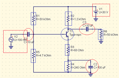
After testing the input and output responses of the transistor for the Common Emitter configuration, the amplifier circuit must be assembled. All passive elements of the circuit must be searched for coupling to the transistor. A DC source is used to polarize the transistor and an AC signal generator to create the input signal of the amplifier. The ground points must be referenced for each source of the circuit and for the Emitter terminal.
Step 5:
The circuit has a polarization known as a voltage divider. Polarization is the analysis of the DC values assumed by the terminals of the transistor so that it can be located in the active region of operation. These values were obtained from the output curve of the common emitter, Ib, IC and Vce.
Step 6:
The polarization by voltage divider, presents a series of equations that allow to calculate the resistance values to design the circuit at the required operation point. Different techniques can be applied to calculate the components of the circuit in DC. The different polarization equations are shown below:
Vb = V1*R5/ (R1+R5)
Re = R3+R4
Ve = Ie*Re
Ic = Ie
Ic = β*Ib
Icsat = V1/ (R2+Re)
Vce = V1-Ic*(R2+Re).
Step 7:
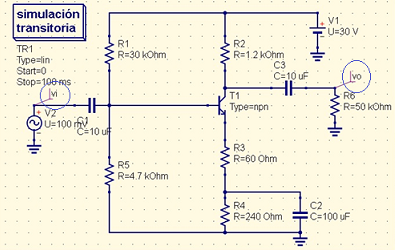
With the calculated values for the resistor and the capacitors, the definitive circuit is configured and an input signal for the audio amplifier of approximately 100mV is also assigned. The capacitors for small signal will behave as coupling elements of the AC input and output signals. The C2 is a capacitor that eliminates the effect of the resistance R4 in AC.
Step 8:
We configure the simulation for a transient response of the circuit, to see the amplification of the input audio signal, a label Vi must be used for the node of the input signal and Vo for the node of the output signal. A transient sweep of 100 ms is assigned.
Step 9:
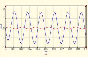
The input signal Vi in red and the output signal Vo in blue, both as a function of time. The gain gain expression has a phase shift between both signals of 180 °, this is due to the negative factor of the gain.
The nextlist code of the audio amplifier with the transistor BJT:
<Components>
<_BJT T1 1 530 230 8 -26 0 0 "npn" 1 "1e-16" 1 "1" 1 "1" 0 "0" 0 "0" 0 "0" 1 "0" 0 "0" 0 "1.5" 0 "0" 0 "2" 0 "100" 1 "1" 0 "0" 0 "0" 0 "0" 0 "0" 0 "0" 0 "0" 0 "0.75" 0 "0.33" 0 "0" 0 "0.75" 0 "0.33" 0 "1.0" 0 "0" 0 "0.75" 0 "0" 0 "0.5" 0 "0.0" 0 "0.0" 0 "0.0" 0 "0.0" 0 "0.0" 0 "26.85" 0 "0.0" 0 "1.0" 0 "1.0" 0 "0.0" 0 "1.0" 0 "1.0" 0 "0.0" 0 "0.0" 0 "3.0" 0 "1.11" 0 "26.85" 0 "1.0" 0>
<GND * 1 370 400 0 0 0 0>
<GND * 1 190 320 0 0 0 0>
<GND * 1 530 500 0 0 0 0>
<GND * 1 650 490 0 0 0 0>
<GND * 1 780 300 0 0 0 0>
<GND * 1 700 160 0 0 0 0>
<Vdc V1 1 700 130 18 -26 0 1 "30 V" 1>
<Vac V2 1 190 290 18 -26 0 1 "100m" 1 "1 GHz" 0 "0" 0 "0" 0>
<R R1 1 370 150 15 -26 0 1 "30 k" 1 "26.85" 0 "0.0" 0 "0.0" 0 "26.85" 0 "US" 0>
<R R5 1 370 370 15 -26 0 1 "7 k" 1 "26.85" 0 "0.0" 0 "0.0" 0 "26.85" 0 "US" 0>
<R R4 1 530 470 15 -26 0 1 "240 Ohm" 1 "26.85" 0 "0.0" 0 "0.0" 0 "26.85" 0 "US" 0>
<R R3 1 530 360 15 -26 0 1 "60 Ohm" 1 "26.85" 0 "0.0" 0 "0.0" 0 "26.85" 0 "US" 0>
<R R2 1 530 130 15 -26 0 1 "1.2 k" 1 "26.85" 0 "0.0" 0 "0.0" 0 "26.85" 0 "US" 0>
<R R6 1 780 270 15 -26 0 1 "50 k" 1 "26.85" 0 "0.0" 0 "0.0" 0 "26.85" 0 "US" 0>
<C C1 1 300 260 -26 17 0 0 "10 uF" 1 "" 0 "neutral" 0>
<C C2 1 650 460 17 -26 0 1 "100 uF" 1 "" 0 "neutral" 0>
<C C3 1 690 240 -26 17 0 0 "10 uF" 1 "" 0 "neutral" 0>
<.TR TR1 1 160 50 0 63 0 0 "lin" 1 "0" 1 "100 ms" 1 "11" 0 "Trapezoidal" 0 "2" 0 "1 ns" 0 "1e-16" 0 "150" 0 "0.001" 0 "1 pA" 0 "1 uV" 0 "26.85" 0 "1e-3" 0 "1e-6" 0 "1" 0 "CroutLU" 0 "no" 0 "yes" 0 "0" 0>
</Components>
<Wires>
<190 260 270 260 "Vi" 230 230 2 "">
<330 230 330 260 "" 0 0 0 "">
<330 230 370 230 "" 0 0 0 "">
<370 230 500 230 "" 0 0 0 "">
<370 180 370 230 "" 0 0 0 "">
<370 230 370 340 "" 0 0 0 "">
<370 100 370 120 "" 0 0 0 "">
<370 100 530 100 "" 0 0 0 "">
<530 160 530 200 "" 0 0 0 "">
<530 260 530 330 "" 0 0 0 "">
<530 390 530 430 "" 0 0 0 "">
<530 430 530 440 "" 0 0 0 "">
<530 430 650 430 "" 0 0 0 "">
<530 200 660 200 "" 0 0 0 "">
<660 200 660 240 "" 0 0 0 "">
<720 240 780 240 "" 0 0 0 "">
<530 100 700 100 "" 0 0 0 "">
<720 240 720 240 "Vo" 750 210 0 "">
</Wires>
<Diagrams>
</Diagrams>
<Paintings>
</Paintings>
The gain expression of the amplifier is approximately 15 of the value of the input signal.
Thank you friends for your attention ... I hope to see you in the next tutorial...
Curriculum
- Qucs simulator for semiconductor electronic circuits: Introduction
- Stages of design of a source regulated with Zener, using QUCS.
Posted on Utopian.io - Rewarding Open Source Contributors
Excellent post. #steemfamilyhi.
Thank you for the contribution. It has been approved.
You can contact us on Discord.
[utopian-moderator]
Hola @edagmi, upv0t3
Este es un servicio gratuito para nuevos usuarios de steemit, para apoyarlos y motivarlos a seguir generando contenido de valor para la comunidad.
<3 Este es un corazón, o un helado, tu eliges .
: )
N0. R4ND0M:
3018 3995 9382 8634
2942 5407 2186 4294
2827 1771 8174 8788
1347 8346 5664 8243
Votado por estar top5 steemfamilyhi
Gracias por el apoyo
Dejando mi apoyo. Saludos hoy estas en el top 5 de #steemfamilyhi. Buen aporte a la comunidad.
Gracias por tu apoyo!!
Felicitaciones, leer esto es como si me hablaras en chino jejeje cambio un bombillo, podría empatar un cable, pero no se nada de Electrónica, Si Admiro mucho la carrera, hace poco una amiga se graduó de ingeniería electrónica en la UCV me consta todo lo que estudio a lo largo de años. Top Five #steemfamilyhi
Muy interesante. Saludos y bendiciones mi apoyo desde #steemfamilyhi
Hey @edagmi I am @utopian-io. I have just upvoted you!
Achievements
Community-Driven Witness!
I am the first and only Steem Community-Driven Witness. Participate on Discord. Lets GROW TOGETHER!
Up-vote this comment to grow my power and help Open Source contributions like this one. Want to chat? Join me on Discord https://discord.gg/Pc8HG9x
Excellent article @edagmi, and thanks for sharing it through utopia.io. I also visit you from the community of #steemfamilyhi. regards
Gran trabajo amigo.Como siempre eres brillante. #steemfamilyhi #top5