Characteristic curves of BJT bipolar junction transistor, using Qucs simulator tools for DC analysis and parameter scanning.
What Will I Learn?
In this tutorial you will learn:
Know the BJT bipolar junction transistors and their characteristic curves.
Analyze the operation of a circuit with transistors, applying two-port networks.
Use the DC Analysis of the Qucs simulator.
Program the parametric sweep of voltage and current values in the Qucs Simulator.
Requirements
- The user must read the previous tutorials, related to the analysis of electronic devices using the Qucs.
- Possess an intermediate knowledge of the management of semiconductor electronic devices of three terminals.
- Know the mode of operation of the BJT transistors and the analysis of circuits with this type of transistors.
Difficulty
- Intermediate
Tutorial Contents
The bipolar junction transistor BJT, is a three-terminal semiconductor device, which has important functions in electronics, it is widely used for the amplification of small signals and the switching of signals to generate digital logic circuits.
The terminals of the transistor are known as Emitter (responsible for generating charge carriers), Base (channel for conducting load carriers) and Collector (Receives charge carriers). They are contaminated semiconductor materials to create two configurations based on their doping. The configurations are PNP where a layer of N-type semiconductor material is placed between two layers of P and NPN semiconductor materials where a layer of type P material is placed between two layers of type N material.
In the following image, the transistor is observed with its three layers, its symbol and its polarization values. For the analysis we are going to polarize a BJT in its active operating region, for this it requires that the junction between the Emitter and the Base be polarized in direct and the union between the Base and the Collector, polarized in inverse.
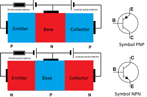
Type N materials are used to contaminate a crystalline Silicon network with atoms of 5 or more valence electrons, which gives a negative charge concentration. P-type materials are used to contaminate a crystalline lattice of pure silicon, with atoms of 3 or less valence electrons, which gives a positive charge concentration.
The BJT transistor is based on two semiconductor junctions that generate a current flow at the Base-Emitter junction input terminals, which allows controlling the output current of the second Base-Collector junction. It has a behavior similar to a current-controlled current source.
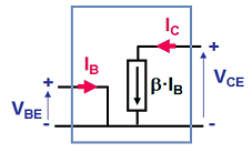
The transistor has a gain factor known as β, and represents the connection of the current of the output terminal as a function of the current of the input terminal, given by the following equation:
Ic = β*Ib
The characteristic curves of the circuit require a sweep of the Base current (Ib), to see the behavior of the output variables, in this case, Collector current (Ic) and Collector Emitter voltage (Vce).
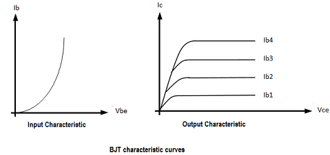
The curves of the transistor are the following:
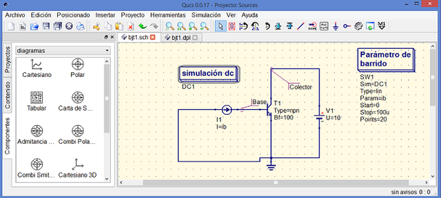
The analysis that we will perform in the Qucs simulator, we can define it as a steady state analysis or DC, this type of analysis calculates the voltage of the circuit nodes and also the derivation currents of the complete circuit. It will also include a sweep of parameters, to generate various families of curves according to the most significant variables of the circuit.
Transistor input characteristic curve:
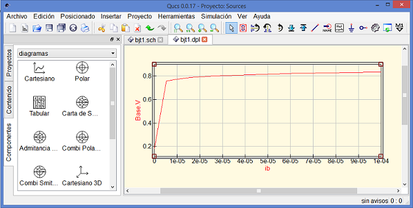
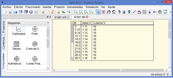
The transistor in its terminals of the input junction behaves like a live polarized diode, that is, the voltage of the diode is maintained for any current value that tends to infinity. In the case of the Base-Emitter junction, the Vbe voltage must be close to 0.8 V for any increase in the base current. To verify this input behavior, we assemble the circuit of the following figure for an NPN transistor, with reference point to ground in the Emitter.
A current source with a parameter ib is used, which will generate a parametric sweep between 0 and 100 μA. The behavior of the Voltage of the Base as a function of the parametric sweep of the Base current is observed in the simulation.
Transistor Output Characteristic Curve:
The output characteristic of the transistor is usually more complex because it includes a third variable in the output graph. The Base current has the function of controlling the characteristic response of the output curve of the transistor, so it must be represented as an output parameter in conjunction with the Collector current and the Collector Emitter voltage.
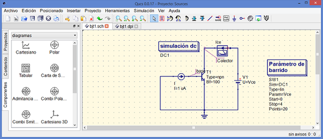
Next, the common Emitter circuit is designed, with a BJT transistor, an independent current source is used to simulate the Base current and to have a variable that is subjected to a parametric sweep to generate the families of transistor curves. The polarization source of the Emitter Collector terminal is also attached. The circuit with the NPN transistor is observed, and the DC analysis is included first to define the polarization values of the transistor.
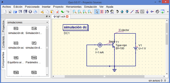
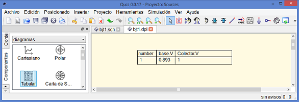
We do a simulation test DC, with the voltage values of the terminal of the Base and of the Collector of the transistor. The Emitter is not measured because it is connected to ground.
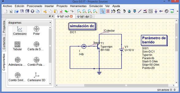
We will place a parametric sweep in order to give different values of the current source and generate the different families of curves. The swept parameter is Ib (the Base current) and is put in the Param property of the parameter sweep and DC1 in the DC simulation.
The simulated results of the parametric sweep of the Base current can be seen in the following table.
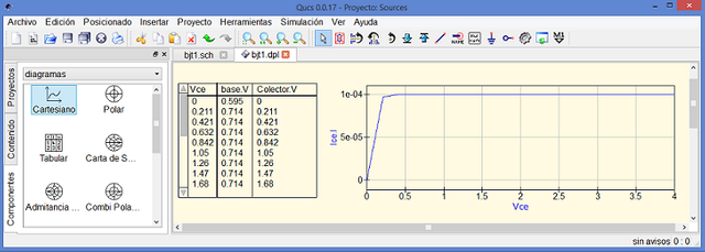
A new sweep of the value of the output current as a function of the Emitter Collector voltage is required, so we must establish the sweep (Vce) and verify the current response of the Collector.
The characteristic curve of the output parameters Ic vs Vce is displayed for a single current value of the Base.
Another parametric sweep must be added to define the variation of the Emitter Collector voltage and to be able to plot the curve of the Collector current, but with the control parameter given by the Base current subjected to the second sweep.
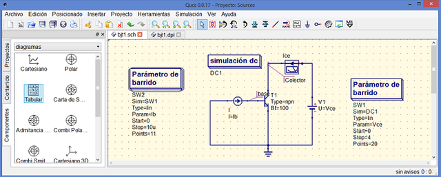
The result must correspond to the family of curves of the BJT NPN transistor, where the control parameter is defined by the current of the Base.
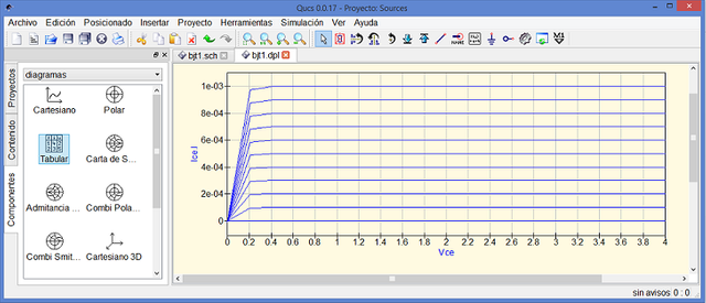
Finally we have got the family of curves of transistor BJT, NPN. This answer is very useful when you need to work with this device to design electronic circuits that handle analog signal amplification procedures.
The netlist code of the schematic circuit for the output characteristic curve of the transistor BJT:
<Components>
<_BJT T1 1 470 180 8 -26 0 0 "npn" 1 "1e-16" 0 "1" 0 "1" 0 "0" 0 "0" 0 "0" 0 "0" 0 "0" 0 "1.5" 0 "0" 0 "2" 0 "100" 1 "1" 0 "0" 0 "0" 0 "0" 0 "0" 0 "0" 0 "0" 0 "0.75" 0 "0.33" 0 "0" 0 "0.75" 0 "0.33" 0 "1.0" 0 "0" 0 "0.75" 0 "0" 0 "0.5" 0 "0.0" 0 "0.0" 0 "0.0" 0 "0.0" 0 "0.0" 0 "26.85" 0 "0.0" 0 "1.0" 0 "1.0" 0 "0.0" 0 "1.0" 0 "1.0" 0 "0.0" 0 "0.0" 0 "3.0" 0 "1.11" 0 "26.85" 0 "1.0" 0>
<GND * 1 470 320 0 0 0 0>
<Idc I1 1 350 180 -26 18 0 0 "ib" 1>
<.DC DC1 1 230 70 0 39 0 0 "26.85" 0 "0.001" 0 "1 pA" 0 "1 uV" 0 "no" 0 "150" 0 "no" 0 "none" 0 "CroutLU" 0>
<IProbe Pr1 1 540 70 -26 -32 0 2>
<Vdc V1 1 600 200 18 -26 0 1 "Vce" 1>
<.SW SW1 1 710 20 0 63 0 0 "DC1" 1 "lin" 1 "Vce" 1 "0" 1 "4" 1 "20" 1>
<.SW SW2 1 30 60 0 63 0 0 "SW1" 1 "lin" 1 "ib" 1 "0" 1 "10u" 1 "11" 1>
</Components>
<Wires>
<600 230 600 310 "" 0 0 0 "">
<470 310 600 310 "" 0 0 0 "">
<470 310 470 320 "" 0 0 0 "">
<470 210 470 310 "" 0 0 0 "">
<600 70 600 170 "" 0 0 0 "">
<470 70 470 150 "" 0 0 0 "">
<440 310 470 310 "" 0 0 0 "">
<440 310 440 320 "" 0 0 0 "">
<220 320 440 320 "" 0 0 0 "">
<220 180 220 320 "" 0 0 0 "">
<220 180 320 180 "" 0 0 0 "">
<380 180 440 180 "Base" 420 150 10 "">
<470 70 510 70 "Colector" 520 110 0 "">
<570 70 600 70 "" 0 0 0 "">
</Wires>
<Diagrams>
</Diagrams>
<Paintings>
</Paintings>
Thank you for your attention, this is a contribution from the @edagmi account to Utopian-io.
Curriculum
- Qucs simulator for semiconductor electronic circuits: Introduction
- Stages of design of a source regulated with Zener, using QUCS.
Posted on Utopian.io - Rewarding Open Source Contributors
@edagmi, Approve is not my ability, but I can upvote you.
UPVOTE!!!!!! #topfive #steemfamilyhi.
use the hash tag for the next occasion
Your contribution cannot be approved because it does not follow the Utopian Rules.
Violated Rules:
Tutorials must be technical instructions that teach non-trivial aspects of an Open Source project.
Same contributions will never be accepted in Utopian twice by the same or different user.
Design or video editing related tutorials, gameplay, simple on-screen instructions, ubiquitous functions (Save, Open, Print, etc.) or basic programming concepts (variables, operators, loops, etc.) will not be accepted.
My Opinion:
You can contact us on Discord.
[utopian-moderator]
Congratulations @edagmi! You have completed some achievement on Steemit and have been rewarded with new badge(s) :
Click on any badge to view your own Board of Honor on SteemitBoard.
To support your work, I also upvoted your post!
For more information about SteemitBoard, click here
If you no longer want to receive notifications, reply to this comment with the word
STOP