The Nano-world: Atomic Layer Deposition
Moore’s Law
In 1965 Gordon Moore made the observation that the number of transistors per unit area on integrated circuits doubled every year. He then made the prediction that this trend would continue on, at least for the foreseeable future. This prediction is called Moore’s Law.
While slowing down slightly, transistor numbers per unit area have doubled every 18 months recently, Moore’s law is still in full effect. However, as we are scaling down we are reaching the physical limits of molecules and atoms. So as we are scaling down to the size of molecules and atoms we also need techniques able to precisely alter the way molecules and atoms interact. This is where Atomic Layer Deposition comes in, which we’ll simply call: ALD.
Chaos to order
ALD is a technique capable of creating a film that is only a couple atoms thick. It is a variation of chemical vapor deposition (CVD), which is a common method for making thin films. This method is especially used in the fabrication of chips. The essence of CVD is that a silicon wafer (a thin slice of semiconductor material) is subjected to precursors in the gas phase, which will react with the silicon wafer and deposit on the surface. These precursors are the gaseous chemicals that react with the silicon wafer; they are ‘precursors’ to the chemical reaction.
Common CVD techniques introduce a mix of precursors to the silicon wafer and this results in a complex system of precursors, byproducts, and other molecular fragments. This is an environment of little control where it’s mostly a matter of chance what is going to be deposited where on the silicon wafer. This has driven scientist to come up with ALD, which benefits from being extremely precise and controllable. How did they achieve this kind of control?
Self-similarity

Figure 1: ALD of silica (SiO2)1
In Figure 1 an example ALD process is shown for silica (silicon dioxide, SiO2). The process of ALD is set up in the same way with a silicon wafer in a reaction chamber. The process starts by introducing a silicon precursor to the chamber. The silicon (Si) precursor reacts with the surface and forms a thin layer. The excess of Si precursor cannot react with itself, which keeps the layer thickness restricted to the size of one Si precursor molecule. After a washing step, a second precursor is introduced. In our case, oxygen (O2) is introduced into the chamber. The O2 reacts with the Si precursor to form SiO2. Just as before the oxygen cannot react with itself and only one precursor layer is added. But now the two precursors have reacted and created a thin SiO2 layer on the surface of the Si wafer. This step-by-step addition combined with flushing steps to wash away reaction byproducts gives ALD superior precision and controllability.
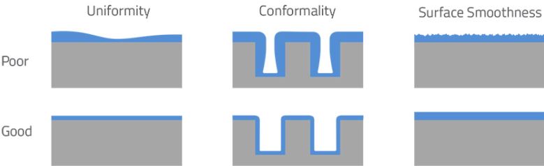
Figure 2: The good and bad of CVD. The ALD variation makes uniform and smooth thin films (blue) that conform to the wafer (grey).1
Therefore the core principle of ALD lies in this inability of precursors to interact with themselves. This self-similarity is the principle of ALD.
Applications
Now that we got through the dry bit, what kind of exciting things does ALD allow us to do?
Microelectronics:
Samsung already started with ALD in the 1990s to improve the capacitor in their DRAM memories. Since then ALD has had a major role in decreasing the size of capacitors. The reason why this is the case is quite complex, but I’ll give it a try to explain it.
Field-effect-transistors, the basis of modern digital integrated circuits, work by using an electric field to allow the flow of electrons between an input (source) and an output (drain). To go from the source to the drain the electrons have to move through a barrier (gate). When a voltage is applied to the source an electric field is developed over the gate. If the electric field is stronger than the gate the electrons are able to flow through the gate. It is very important that this gate is highly uniform and free of any holes, otherwise, leakage would happen all over the place. Let is so happen that smoothness and uniformity is the strong suit of ALD.
ALD allows the deposition of highly gate-suitable materials in exactly the right way: smooth and uniform. Intel has been able to reduce their transistor structure from 65 nm to 22 nm by using ALD. As electronics keep scaling down ALD will become an even more critical tool for this industry.
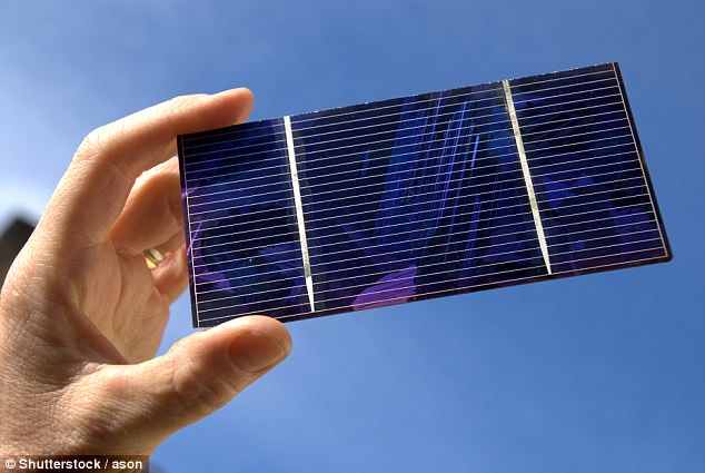
Photovoltaics:
Solar cell development is the business of interface engineering. The right material properties of interfaces and subsequent interaction between these interfaces is a key factor in the photovoltaic industry. As discussed before, ALD is a technique capable of creating precise and highly controllable surfaces. It is therefore ideal for the design of solar cells. If you are more interested in the application of ALD for the photovoltaic industry I recommend this article, since a detailed explanation would be quite dense.
Energy storage:
Next-generation fuel cells are in the making. One variant of fuel cells converts chemical energy to electric energy. These fuel cells are called solid oxide fuel cells (SOFCs). SOFCs consist of three layers: a porous anode material, an ion conducting electrolyte, and a cathode material. All three of these layers benefit from ALD. To focus a bit on the electrolyte, its function is to transfer oxide ions from the cathode to the anode. Using ALD to shrink this electrolyte layer it decreases the length these ions have to travel and the resistance of the electrolyte layer. This allows for a more rapid ion transfer giving a better performance. For more information on SOFCs I recommend this article.
I hope this post wasn’t too dense and you were all able to follow it. Once you scale down into the nanometers things have a tendency to become quite complex as you are no longer dealing with continuum mechanics but with separate molecules and atoms. If it was too much of a hassle to get through then please let me know. Have a nice day!
References:
Moore’s Law
Chemistry at the bottom: Atomic layer deposition
Tech Brief: A Look at Atomic Layer Deposition (ALD)
Atomic Layer Deposition: An Overview
A brief review of atomic layer deposition: From fundamentals to applications
Field-effect transistors
Atomic layer deposition for photovoltaics
Solid Oxide Fuel Cells
Images by:
wccftech
Recently from @Altherion
Printing ‘Living Matter’
The Lost Atmosphere
A Killer in Space
Errors of experimentation
Total Daily Energy Expenditure
2017 – Obesity update

To answer your question: this post was not too dense. I really liked it! (but I have no intelligent comment to make :p)
Thank you @lemouth. I appreciate the feedback!
Even though I only understood just over half of that, I really enjoyed reading that! Ima follow you for more!
Thanks for the feedback, I appreciate it!