How to make a VFD clock step by step
Hello, friends! I decided to publish this material under the motto of electronics DIY, i.e. do it yourself. I very much hope that there will be more such posts, as well as authors who write on this subject. Now there are not so many, maybe not the format on this resource, but I hope they will be more.
Next, I'll talk about how I made the VFD clock and of course there will be a detailed story about how to do it myself.
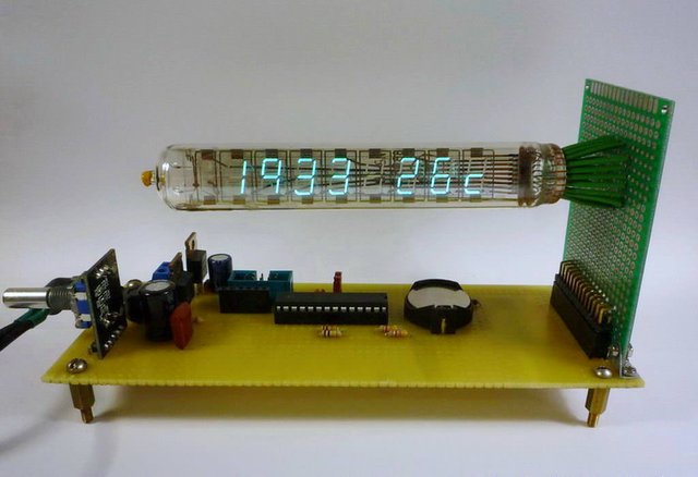
This is the first version of the watch and that's what they can:
- Display both alternately and static: time, date, day, month name, year, show the temperature of the air.
- Have a brightness adjustment.
- Ability to specify the format of output date and time.
- Have a timer.
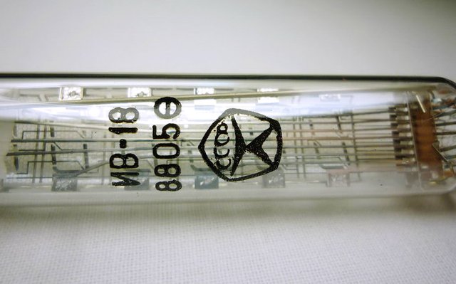
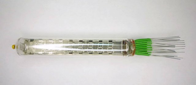
I did this watch for my son, and it was very interesting for me. Since this is a hobby for me, I did not make quickly, but slowly and with pleasure. It all started with the search for the IV-18 tube, this was found on Ebay. To my surprise, the seller turned out to be from Russia, so parcel came in the shortest time.
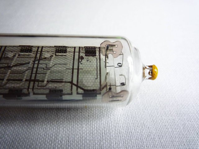
Look at the IV-18 tube closer, it works on VFD technology.
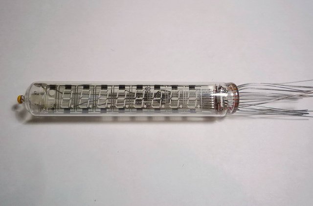
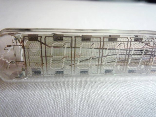
Technical information about the indicator
The digital multi-digit vacuum fluorescent (VFD) indicator is designed to display information in the form of digits from 0 to 9 and a decimal place in each of 8 digital digits.
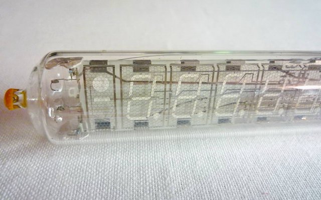
VFD is an electrovacuum triode of direct glow with a lot of phosphor-coated anodes. Lamp parameters are chosen so that it can work at low anode voltages - from 27 to 50 V.
The cathode is a direct filament cathode made of tungsten with addition of 2% thorium to facilitate emission at a relatively low temperature.
In the indicator there are two parallel filaments with a diameter less than a human hair. For their tension, small flat springs are used. The filament voltage ranges from 4.3 to 5.5 V.
VFD grids are flat. The number of grids is equal to the amount of familiarity of the indicator. The purpose of the grids is twofold: first, they reduce the voltage sufficient for the indicator to glow brightly, and secondly, provide the possibility of switching discharges during dynamic indication.
The anodes are coated with a phosphor with a low excitation energy of only a few electron volts. It is this fact that allows the tube to work at low anode voltage.
Technical parameters IV-18
- Glow Color: Green
- Heating voltage: 4.3-5.5 V
- Current of heating: 85 ± 10 mA
- Anode-segment voltage pulse: 50 V
- The greatest voltage of the anodes-segments: 70 V
- The largest current of the anode-segment: 1.3 mA
- Current anodes-segments pulse total: 40 mA
- Pulse grid voltage: 50 V
- The largest grid voltage pulse: 70 V
- Minimum operating time: 10,000 h
Dimensions
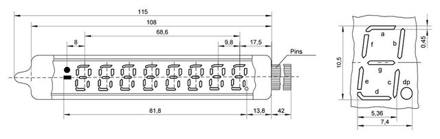
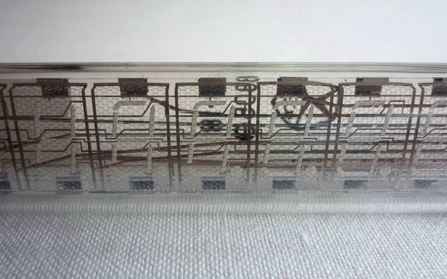
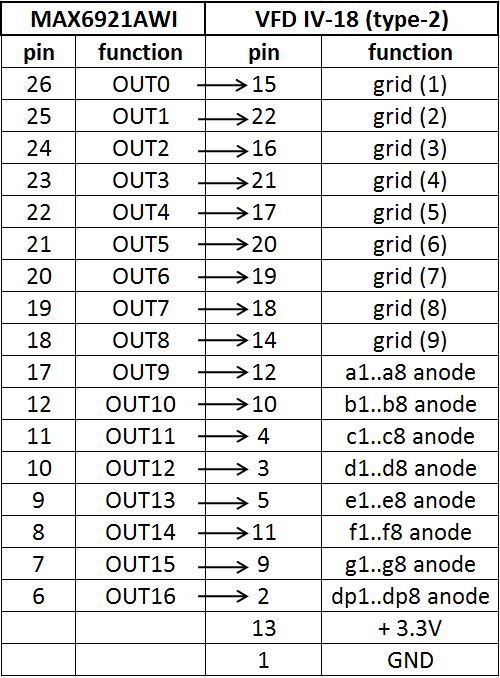
Pin mapping IV-18 (type-2)
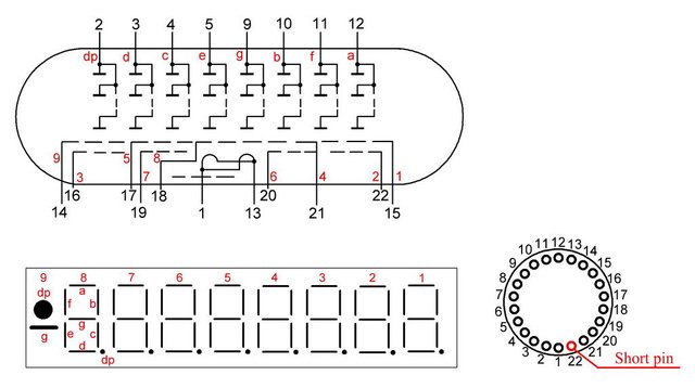
1 - Cathode;
2 - dp1 ... dp8 - anodes-segments with the 1st to the 8th digit;
3 - d1 ... d8 - anodes-segments with the 1st to the 8th digit;
4 - c1 ... c8 - anodes-segments with the 1st to the 8th digit;
5 - e1 ... e8 - anodes-segments with the 1st to the 8th digit;
6 - Do not connect (free);
7 - Do not connect (free);
8 - Do not connect (free);
9 - g1 ... g8 - anodes-segments with the 1st to the 8th digit;
10 - b1 ... b8 - anodes-segments with the 1st to the 8th digit;
11 - f1 ... f8 - anodes-segments with the 1st to the 8th digit;
12 - a1 ... a8 - anodes-segments with the 1st to the 8th digit;
13 - Cathode;
14 - Grid of the 9th digit;
15 - Grid of the 1th digit;
16 - Grid of the 3th digit;
17 - Grid of the 5th digit;
18 - Grid of the 8th digit;
19 - Grid of the 7th digit;
20 - Grid of the 6th digit;
21 - Grid of the 4th digit;
22 - Grid of the 2th digit;
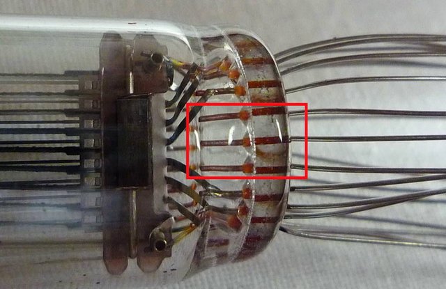
Information about pin mapping assignments is valid only for the IV-18 (type-2) tube. There is also a type-1, but how to understand what kind of tube will you have ?! It's simple! Based on the description, pins 6, 7, 8 are not connected! This is very clearly seen in the photo.
Electrical circuit
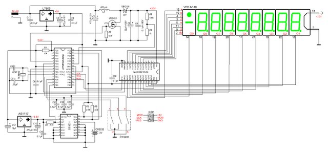
I duplicate the scheme on DropBox in the maximum resolution. There will also be a file with firmware.
Next, I'll explain in detail how the circuit works.
1. Microcontroller
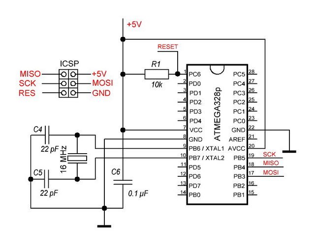
The clock is controlled by the microcontroller Atmega328P-PU in the DIP package, it controls the indicator driver and the anode voltage block, receives data from the "clock" chip, and also an encoder for controlling the clock is connected to it. Be careful, when used in the TQFP case, the pinout will be different. If you want, you can replace Atmega328P-PU with Atmega168PA, there is enough memory, but I took it with a margin for future firmware (at the moment it is 11.8 Kb). Also, instead of the microcircuit microcircuit, you can use Arduino, in this case you need to watch the pin mapping. In this diagram, the Atmega connection is typical, it operates at a frequency of 16 MHz from an external quartz resonator. Accordingly fuse equal:
Low Fuse 0xFF, High Fuse 0xDE, Extended Fuse 0x05. Reset is pulled up to positive power through the resistor. After correctly installing the fuse, the firmware was downloaded via the ICSP connector (SCK, MOSI, MISO, RESET, GND, Vcc).
2. Power
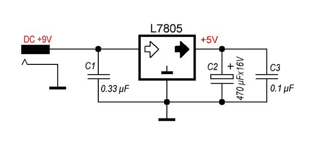
The input voltage of 9V goes to the linear regulator L7805 and goes down to 5V. This voltage is necessary for powering the "digital logic", it goes to the microcontroller and driver MAX6921. Because our microcontroller operates at 16 MHz, then the recommended voltage (based on the datasheet) is 5V.
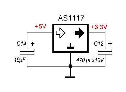
The circuit also needs 3.3 V power, for this I applied AS1117. This voltage is applied to the DS3231 chip.
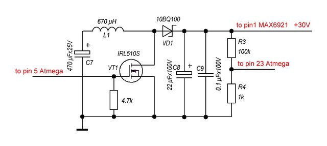
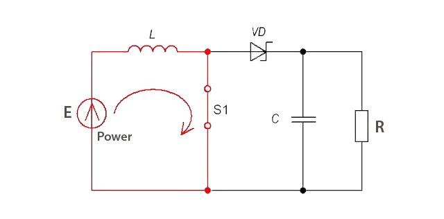
To obtain the anode voltage, a simple step-up converter circuit is used, which consists of the inductance L1, the IRL510S transistor, the Schottky diode 10BQ100, and the capacitor C8. I'll try to explain how this works, for this purpose we will present the scheme in the form:
First step
Second step
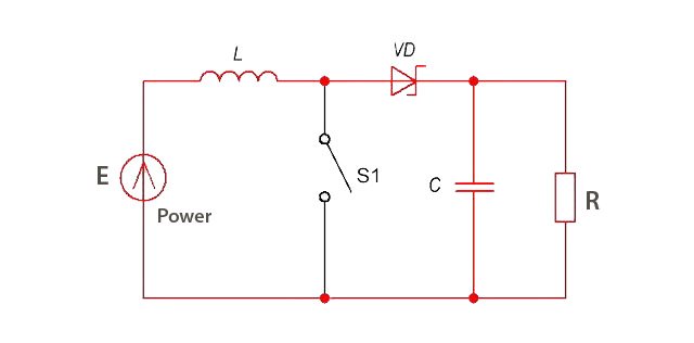
The converter operates in two stages. Imagine that the transistor VT1 acts as the key S1. At the first stage the transistor is open (the key is closed), the current from the source passes through the inductance L, in the core of which the energy is stored in the form of a magnetic field. At the second stage, the transistor is closed (the switch is open), the stored energy in the coil begins to be released, and the current tends to be maintained at the same level as when the key was opened. As a result, the voltage in the coil jumps abruptly, passes through the diode VD and accumulates in the capacitor C. Then, the key closes again, and the coil starts to receive energy again, while the load operates from the capacitor C, and the diode VD does not allow the current to return to the source power supply. The stages are repeated one by one, preventing the capacitor from "emptying".
The transistor is controlled by the PWM from the microcontroller, thereby changing the charging time of the capacitor C. The longer the charge time, the higher the voltage on the load. The Internet has a calculator for calculating the output voltage, depending on the frequency of the PWM, inductance and capacitance.
Resistors R3 and R4 are a divider, the voltage from which is fed to the analog-to-digital converter (ADC) of the microcontroller. This is necessary to control the voltage at the anodes (not more than 70 V allowed) and brightness control. Information about the anode voltage is output to the indicator in one of the operating modes.
3. Clock Microchip
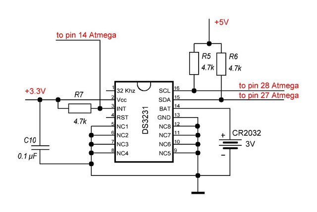
As a real-time clock, the DS3231 chip from Dallas Semiconductor is used. This is a high-precision real-time clock (RTC) with built-in I2C interface, a thermocompensated quartz oscillator and a quartz resonator in one enclosure. The battery CR2032 serves as a backup power source so that the watch does not reset when the power is turned off.
4. Encoder
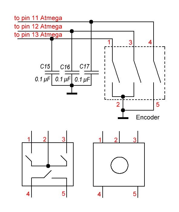
In this scheme, an incremental encoder is used to adjust the clock and select the operating mode. It is desirable to use the built-in clock button. The principle of operation is that the encoder produces pulses ("ticks") when the knob is turned. Our task is to catch these "ticks" through the microcontroller. In this case, a short-circuit to earth occurs. To suppress the chatter of the contacts, internal pull-up resistors are used, as well as 0.1 μF capacitors.
5. Tube driver
Indicator IV-18 is a radiolamp - triode with a cathode of direct glow, control grids (working from the "plus" power) and a bunch of anodes with a luminescent coating. Above each group of anode segments (a, b, c, d, e, f, g) is a separate grid.
The principle of indicating the digit of one of the digits is that the electric field of the control grid accelerates the electrons, which, flying through a rare grid, reach those anode-segments to which the anode voltage is applied. Electrons, falling on a phosphor, cause its luminescence.
To output a single-digit digit, it is enough to apply voltage to the corresponding anodes-segments and grid. This will be a static indication. To light all the digits in each digit, you need to use dynamic indication, because the anodes-segments in all the same discharges are interconnected and have general conclusions. The grid for each digit has its own separate output.
Manage the anodes-segments and grids can be assembled from transistor keys, and can be a special microcircuit driver MAX6921AWI.
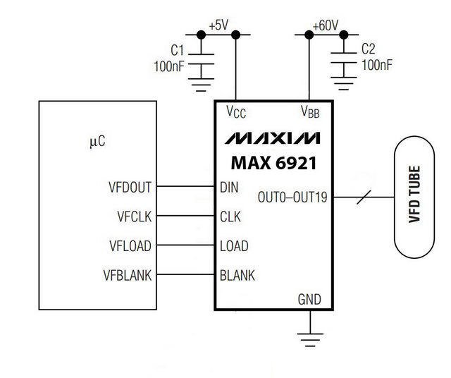
The microcircuit is a high-voltage shift register that has 20 outputs with a permissible voltage of 76 V and a current of up to 45 mA. Data input is via a serial interface. CLK - clock input, DIN - serial data entry, LOAD - data download, BLANK - output switching, DOUT - is intended for cascading of the same chips. BLANK pulls to the ground, i.e. the driver will be permanently turned on.
The principle of operation of the MAX6921 is similar to the operation of the shift register 74HC595. When a logical unit appears at the clock input CLK, the register reads the bit from the data input Din and writes it to the lowest bit. When the next pulse arrives at the clock input, everything repeats, only the bit written earlier is shifted to one bit (starting from OUT19 to OUT0), and the newly arrived bit occupies its place. When all 20 bits are full and the twenty-first clock pulse arrives, the register starts to fill up again from the low order and everything repeats again. In order for data to appear at OUT0 ... OUT19, you need to feed a logical unit to the LOAD input.
There is one nuance with the MAX6921AWI chip, there is a similar MAX6921AUI - it has a completely different pinout !!!
I will give the table of correspondence of the driver and indicator outputs, so it's easier and more comprehensible to collect than to monitor the electrical connections on the circuit.
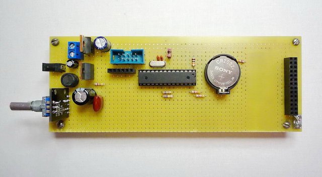
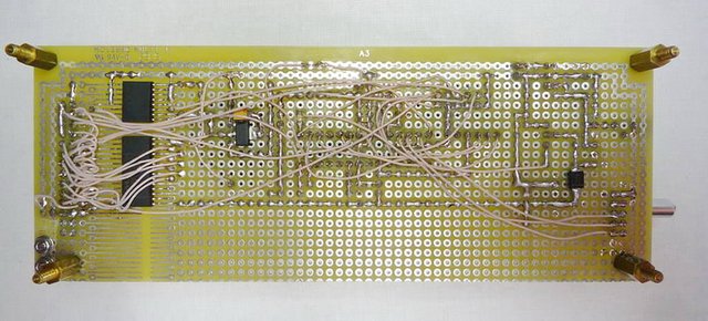
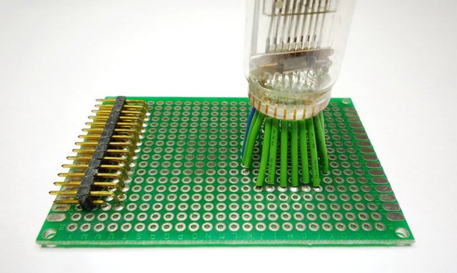
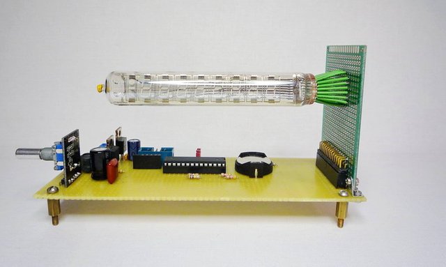
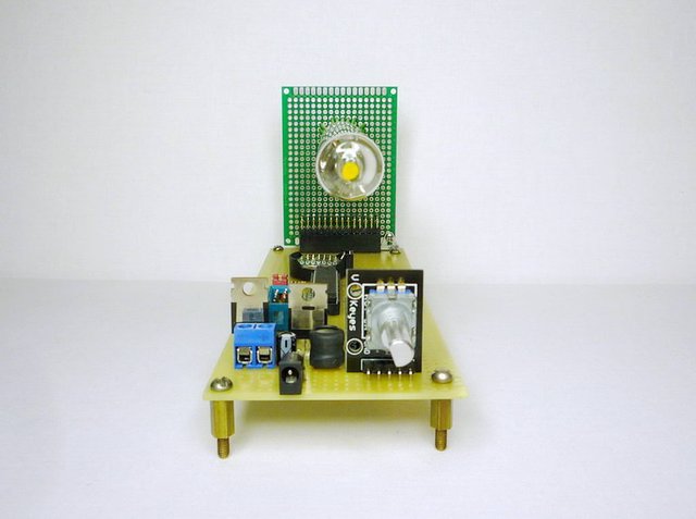
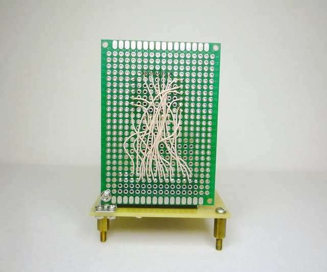
I want to show a few photos of how I did it
I'll show you some video how it works
▶️ DTube
▶️ IPFS
This is all friends, told and showed everything in detail. I hope I did not tire out the theory, and I apologize if I did not describe it very competently. Ready to answer all questions in the comments.
With the best wishes, @gleb-jeglov aka Evgeny!
Крутые часики! Впечатлен)
Оу, спасибо!
Thank you very much for giving you such a beautiful post. We are so lucky that you have a genius like you
Oh .. praise me)) Thank you !! I think, at desire so everyone can make =)
Nice project. I see that the tube is from CCCP, which means that the tube might last long time. I never had a chance to get into VFDs, I'd make project like this out of ordinary 7-segment displays with some digital logic chips.
Keep up the good work!
Man, VFD tube IV-18 and others can be bought on Ebay with the world delivery =)
It's more like I don't have powerful enough power supply to play around with VFDs
You need to make a step-up converter, I'll tell you how to do it in the next posts;)
I know. I will need a couple of boost converters. I'm saying, I don't have lab bench power supply, I don't know if my self made PSU will handle it.
This seems to almost be a copy of an article in 2009 by Jason von Nieda or have I missed something. The code is very old as the 'send' function has been renamed write etc.