Solid state physics: Basic Theory of Semiconductors 1st part
1.- Semiconductor
Semiconductors are defined as "crystalline substances that have an energy band structure in which a band of electronic states, completely filled at a temperature of 0 k, is separated from one that is completely empty at absolute zero, by means of a region narrow forbidden energy".

Every semiconductor at 0 K is a perfect insulator. Because all the electronic states are in the same band that is completely full at 0 K, and there are no states available for electrical conduction to occur in the presence of an electric field.
The statistical distribution of electronic states in semiconductors is governed by the statistical distribution function of Fermi-Dirac (F-D). The function of FD is a step function at 0 K, and therefore all electronic states are occupied below the Fermi energy. Above the Fermi energy at 0K all electronic states are unoccupied.
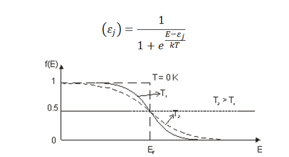
Figure 1. Equation and statistical function Fermi-Dirac.
At temperatures above 0 K, the statistical distribution function of FD forces occupied electronic states to exist above the Fermi energy. These new occupied states appear in the next band that was empty. This band is called the driving band. The band that was previously fully filled is called the valence band.
Thus at temperatures other than 0 K, these new states occupied in the driving band have many other states available in the same band; that allows them to generate an electric current in the presence of an electric field. At the same time, in the valence band at temperatures other than 0 K, there are electronic states that are no longer occupied. These unoccupied electronic states allow the generation of an electric current in the presence of the electric field. This is an important characteristic of semiconductors, in which the current not only comes from the electronic states in the conduction band, but also the electronic states in the valence band, also contribute to generate an electric current. As a consequence of this, in semiconductors currents are usually greater than in metals in the presence of an electric field.
This description corresponds to that of a perfect intrinsic semiconductor. Where there is only one valence band and one conduction band separated by a region of forbidden energy, known as the forbidden semiconductor energy gap.
2.- Energy Bands
2.1.- Prohibited Energy Gap
In section 1, semiconductors were described in terms of a band of accessible states that are fully filled to 0 K. This is the so-called valence band. Above the valence band is the driving band. Between the valence band and conduction band there is a region of energy where there are no accessible states. In this region called the forbidden energy gap and denoted as Eg, there are no accessible states because there are no solutions allowed to the Schrödinger equation in this energy range. This means that no electron can have these energy values.
The forbidden energy gap is a particular feature of each semiconductor. The values of the forbidden gap are in the range of 0.1 eV to 5 eV. The larger the value of the forbidden gap, the more insulating the semiconductor will behave.
This described scheme of valence band, conduction band and forbidden energy region, is what is called the band structure of a semiconductor. The scheme of the band structure, in the phase space of E versus K, is shown in Figure 2. The forbidden energy gap is shown by the shaded area in light gray.
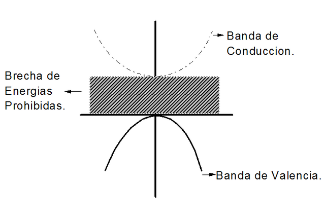
Figure 2. Schematic representation of a band structure of a semiconductor.
2.2.- Direct and Indirect Gaps
The x-axis in Figure 2 represents the vectors of the reciprocal space (K) in the first Brillouin zone. Transitions between electronic states usually occur at the same value of K. In this type of transitions there are no changes at the moment. The solutions to the Schrödinger equation in a crystal can result in a very complex band structure. But, whenever the prohibited energy gap is defined, the minimum gap between the valence band and the driving band is taken as reference.
In many cases, the valence band maximum is found at the same value of K, which is the minimum of the conduction band. When this happens, it is said that the forbidden energy gap is a direct breach.
When the maximum of the valence band is not located at the same value of K as the minimum of the conduction band, it is said that the energy gap is an indirect gap. In this case, when an electronic transition occurs between the valence band and conduction band, the participation of a phonon, which assumes the moment difference, is necessary.
Figure 3 shows the cases of band structures for a direct gap semiconductor (a) and indirect gap (b).
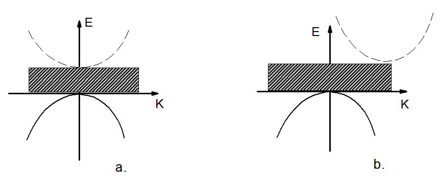
Figure 3. Gaps of direct and indirect energy.
Bibliography:
- Kittel, C. (1995). Introduction to solid state physics.